- 您现在的位置:买卖IC网 > PDF目录231009 > S29JL032H60TAI023 (ADVANCED MICRO DEVICES INC) 2M X 16 FLASH 3V PROM, 60 ns, PDSO48 PDF资料下载
参数资料
| 型号: | S29JL032H60TAI023 |
| 厂商: | ADVANCED MICRO DEVICES INC |
| 元件分类: | PROM |
| 英文描述: | 2M X 16 FLASH 3V PROM, 60 ns, PDSO48 |
| 封装: | MO-142DD, TSOP-48 |
| 文件页数: | 24/66页 |
| 文件大小: | 1691K |
| 代理商: | S29JL032H60TAI023 |
第1页第2页第3页第4页第5页第6页第7页第8页第9页第10页第11页第12页第13页第14页第15页第16页第17页第18页第19页第20页第21页第22页第23页当前第24页第25页第26页第27页第28页第29页第30页第31页第32页第33页第34页第35页第36页第37页第38页第39页第40页第41页第42页第43页第44页第45页第46页第47页第48页第49页第50页第51页第52页第53页第54页第55页第56页第57页第58页第59页第60页第61页第62页第63页第64页第65页第66页
28
S29JL032H
S29JL032H_00A11 March 10, 2005
Advan ce
In form ati o n
This device enters the CFI Query mode when the system writes the CFI Query
command, 98h, to address 55h in word mode (or address AAh in byte mode), any
time the device is ready to read array data. The system can read CFI information
must write the reset command.The CFI Query mode is not accessible when the
device is executing an Embedded Program or embedded Erase algorithm.
The system can also write the CFI query command when the device is in the au-
toselect mode. The device enters the CFI query mode, and the system can read
command to reading array data.
For further information, please refer to the CFI Specification and CFI Publication
100. Contact your local sales office for copies of these documents.
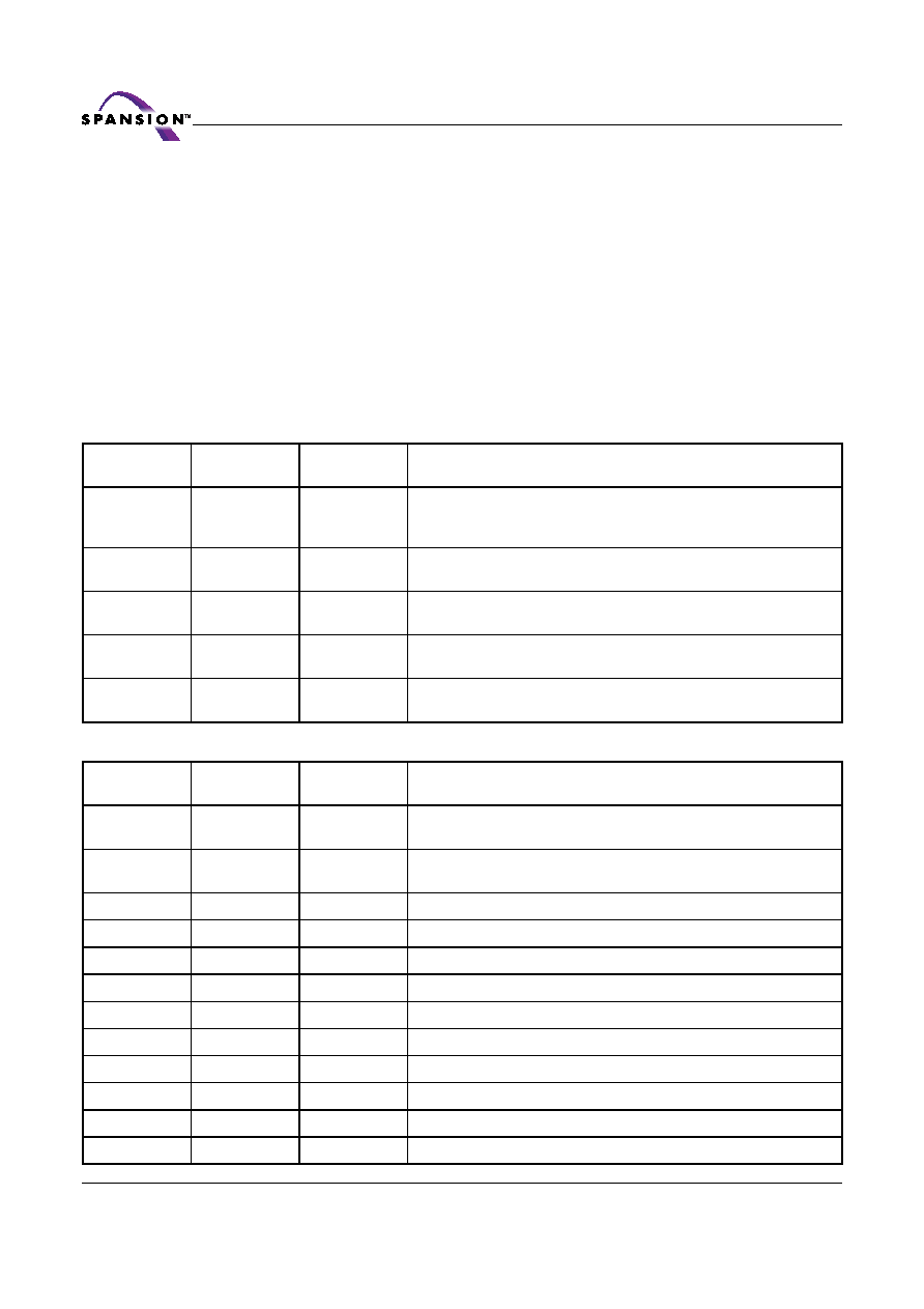
Table 9. CFI Query Identification String
Table 10. System Interface String
Addresses
(Word Mode)
Addresses
(Byte Mode)
Data
Description
10h
11h
12h
20h
22h
24h
0051h
0052h
0059h
Query Unique ASCII string “QRY”
13h
14h
26h
28h
0002h
0000h
Primary OEM Command Set
15h
16h
2Ah
2Ch
0040h
0000h
Address for Primary Extended Table
17h
18h
2Eh
30h
0000h
Alternate OEM Command Set (00h = none exists)
19h
1Ah
32h
34h
0000h
Address for Alternate OEM Extended Table (00h = none exists)
Addresses
(Word Mode)
Addresses
(Byte Mode)
Data
Description
1Bh
36h
0027h
VCC Min. (write/erase)
D7–D4: volt, D3–D0: 100 millivolt
1Ch
38h
0036h
VCC Max. (write/erase)
D7–D4: volt, D3–D0: 100 millivolt
1Dh
3Ah
0000h
VPP Min. voltage (00h = no VPP pin present)
1Eh
3Ch
0000h
VPP Max. voltage (00h = no VPP pin present)
1Fh
3Eh
0003h
Typical timeout per single byte/word write 2N s
20h
40h
0000h
Typical timeout for Min. size buffer write 2N
s (00h = not supported)
21h
42h
0009h
Typical timeout per individual block erase 2N ms
22h
44h
0000h
Typical timeout for full chip erase 2N ms (00h = not supported)
23h
46h
0005h
Max. timeout for byte/word write 2N times typical
24h
48h
0000h
Max. timeout for buffer write 2N times typical
25h
4Ah
0004h
Max. timeout per individual block erase 2N times typical
26h
4Ch
0000h
Max. timeout for full chip erase 2N times typical (00h = not supported)
相关PDF资料 |
PDF描述 |
|---|---|
| S29AL016D70BAI022 | 1M X 16 FLASH 3V PROM, 70 ns, PBGA48 |
| S29AL016D70TAN013 | 1M X 16 FLASH 3V PROM, 70 ns, PDSO48 |
| S29AL016D90BFN013 | 1M X 16 FLASH 3V PROM, 90 ns, PBGA48 |
| SRL91-17UGR2-BB99 | ROCKER SWITCH, SPDT, MOMENTARY, PANEL MOUNT |
| SRL91-13AAR2-BB99 | ROCKER SWITCH, SPDT, LATCHED, PANEL MOUNT |
相关代理商/技术参数 |
参数描述 |
|---|---|
| S29JL032H60TAI210 | 制造商:SPANSION 制造商全称:SPANSION 功能描述:32M BIT CMOS 3.0V FLASH MEMORY |
| S29JL032H60TAI211 | 制造商:SPANSION 制造商全称:SPANSION 功能描述:32M BIT CMOS 3.0V FLASH MEMORY |
| S29JL032H60TAI212 | 制造商:SPANSION 制造商全称:SPANSION 功能描述:32M BIT CMOS 3.0V FLASH MEMORY |
| S29JL032H60TAI213 | 制造商:SPANSION 制造商全称:SPANSION 功能描述:32M BIT CMOS 3.0V FLASH MEMORY |
| S29JL032H60TAI220 | 制造商:SPANSION 制造商全称:SPANSION 功能描述:32M BIT CMOS 3.0V FLASH MEMORY |
发布紧急采购,3分钟左右您将得到回复。