- 您现在的位置:买卖IC网 > PDF目录192305 > S71GL064A04BAW0F3 (Spansion Inc.) Stacked Multi-Chip Product (MCP) Flash Memory and RAM PDF资料下载
参数资料
| 型号: | S71GL064A04BAW0F3 |
| 厂商: | Spansion Inc. |
| 英文描述: | Stacked Multi-Chip Product (MCP) Flash Memory and RAM |
| 中文描述: | 堆叠式多芯片产品(MCP)的闪存和RAM |
| 文件页数: | 50/102页 |
| 文件大小: | 1606K |
| 代理商: | S71GL064A04BAW0F3 |
第1页第2页第3页第4页第5页第6页第7页第8页第9页第10页第11页第12页第13页第14页第15页第16页第17页第18页第19页第20页第21页第22页第23页第24页第25页第26页第27页第28页第29页第30页第31页第32页第33页第34页第35页第36页第37页第38页第39页第40页第41页第42页第43页第44页第45页第46页第47页第48页第49页当前第50页第51页第52页第53页第54页第55页第56页第57页第58页第59页第60页第61页第62页第63页第64页第65页第66页第67页第68页第69页第70页第71页第72页第73页第74页第75页第76页第77页第78页第79页第80页第81页第82页第83页第84页第85页第86页第87页第88页第89页第90页第91页第92页第93页第94页第95页第96页第97页第98页第99页第100页第101页第102页
March 31, 2005 S71GL032A_00_A0
S71GL032A Based MCPs
51
Advance
Informatio n
After the Program Resume command is written, the device reverts to program-
ming. The system can determine the status of the program operation using the
DQ7 or DQ6 status bits, just as in the standard program operation. See Write Op-
eration Status for more information.
The system must write the Program Resume command (address bits are don’t
care) to exit the Program Suspend mode and continue the programming opera-
tion. Further writes of the Resume command are ignored. Another Program
Suspend command can be written after the device has resumed programming.
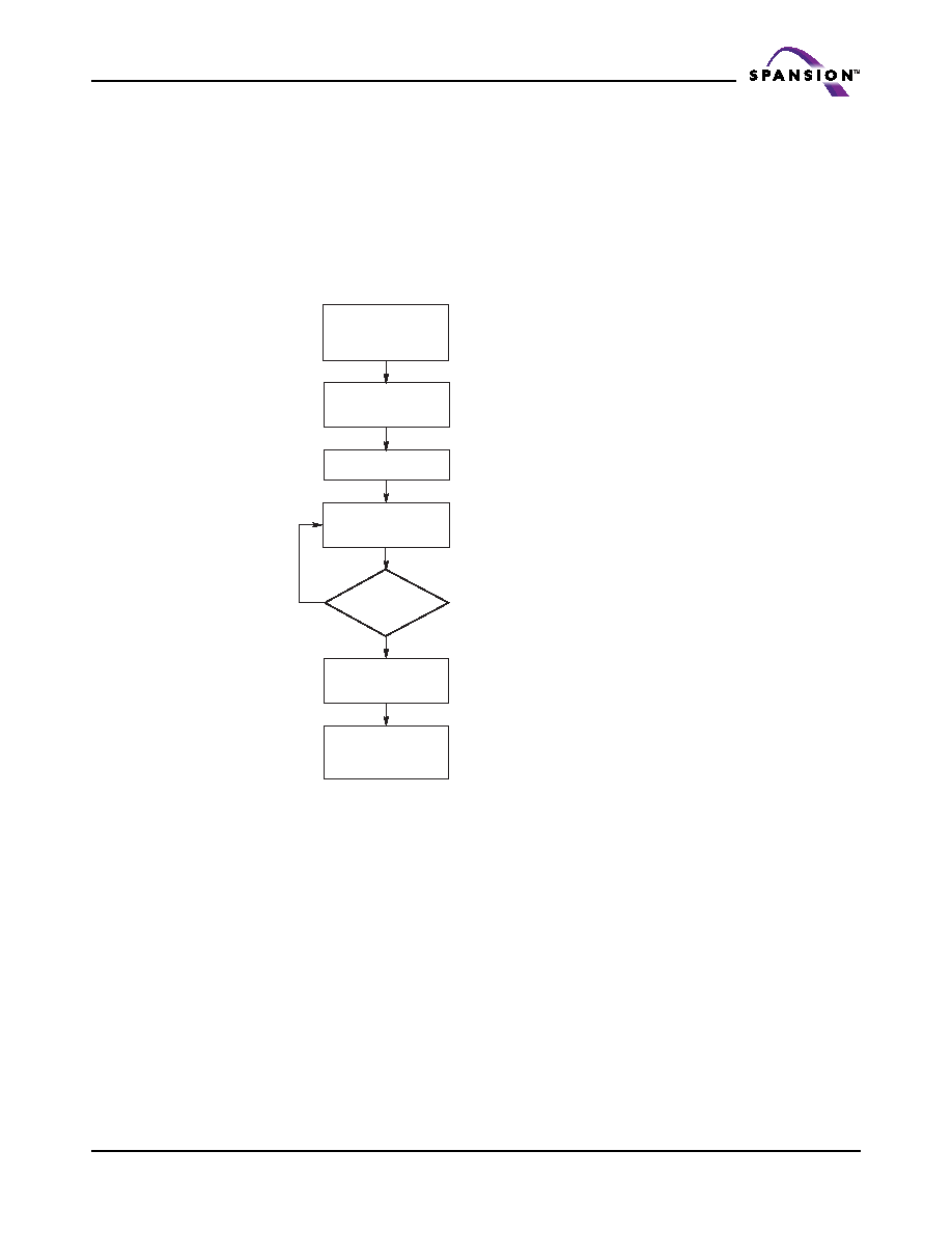
Figure 5. Program Suspend/Program Resume
Chip Erase Command Sequence
Chip erase is a six bus cycle operation. The chip erase command sequence is ini-
tiated by writing two unlock cycles, followed by a set-up command. Two
additional unlock write cycles are then followed by the chip erase command,
which in turn invokes the Embedded Erase algorithm. The device does not require
the system to preprogram prior to erase. The Embedded Erase algorithm auto-
matically preprograms and verifies the entire memory for an all zero data pattern
prior to electrical erase. The system is not required to provide any controls or tim-
ings during these operations. Table 22 shows the address and data requirements
for the chip erase command sequence.
When the Embedded Erase algorithm is complete, the device returns to the read
mode and addresses are no longer latched. The system can determine the status
of the erase operation by using DQ7, DQ6, or DQ2. Refer to the Write Operation
Status section for information on these status bits.
Program Operation
or Write-to-Buffer
Sequence in Progress
Write Program Suspend
Command Sequence
Command is also valid for
Erase-suspended-program
operations
Autoselect and SecSi Sector
read operations are also allowed
Data cannot be read from erase- or
program-suspended sectors
Write Program Resume
Command Sequence
Read data as
required
Done
reading?
No
Yes
Write address/data
XXXh/30h
Device reverts to
operation prior to
Program Suspend
Write address/data
XXXh/B0h
Wait 15
s
相关PDF资料 |
PDF描述 |
|---|---|
| S71GL064A04BFI0B2 | Stacked Multi-Chip Product (MCP) Flash Memory and RAM |
| S71GL064A04BFI0B3 | Stacked Multi-Chip Product (MCP) Flash Memory and RAM |
| S71GL064A04BFI0F3 | Stacked Multi-Chip Product (MCP) Flash Memory and RAM |
| S71GL064A04BFI0F2 | Stacked Multi-Chip Product (MCP) Flash Memory and RAM |
| S71GL064A04BFW0B2 | Stacked Multi-Chip Product (MCP) Flash Memory and RAM |
相关代理商/技术参数 |
参数描述 |
|---|---|
| S71GL064A04BFI0B0 | 制造商:SPANSION 制造商全称:SPANSION 功能描述:Stacked Multi-Chip Product (MCP) Flash Memory and RAM |
| S71GL064A04BFI0B2 | 制造商:SPANSION 制造商全称:SPANSION 功能描述:Stacked Multi-Chip Product (MCP) Flash Memory and RAM |
| S71GL064A04BFI0B3 | 制造商:SPANSION 制造商全称:SPANSION 功能描述:Stacked Multi-Chip Product (MCP) Flash Memory and RAM |
| S71GL064A04BFI0F0 | 制造商:SPANSION 制造商全称:SPANSION 功能描述:Stacked Multi-Chip Product (MCP) Flash Memory and RAM |
| S71GL064A04BFI0F2 | 制造商:SPANSION 制造商全称:SPANSION 功能描述:Stacked Multi-Chip Product (MCP) Flash Memory and RAM |
发布紧急采购,3分钟左右您将得到回复。