- 您现在的位置:买卖IC网 > PDF目录192305 > S71GL064A04BAW0F3 (Spansion Inc.) Stacked Multi-Chip Product (MCP) Flash Memory and RAM PDF资料下载
参数资料
| 型号: | S71GL064A04BAW0F3 |
| 厂商: | Spansion Inc. |
| 英文描述: | Stacked Multi-Chip Product (MCP) Flash Memory and RAM |
| 中文描述: | 堆叠式多芯片产品(MCP)的闪存和RAM |
| 文件页数: | 86/102页 |
| 文件大小: | 1606K |
| 代理商: | S71GL064A04BAW0F3 |
第1页第2页第3页第4页第5页第6页第7页第8页第9页第10页第11页第12页第13页第14页第15页第16页第17页第18页第19页第20页第21页第22页第23页第24页第25页第26页第27页第28页第29页第30页第31页第32页第33页第34页第35页第36页第37页第38页第39页第40页第41页第42页第43页第44页第45页第46页第47页第48页第49页第50页第51页第52页第53页第54页第55页第56页第57页第58页第59页第60页第61页第62页第63页第64页第65页第66页第67页第68页第69页第70页第71页第72页第73页第74页第75页第76页第77页第78页第79页第80页第81页第82页第83页第84页第85页当前第86页第87页第88页第89页第90页第91页第92页第93页第94页第95页第96页第97页第98页第99页第100页第101页第102页
84
S71GL032A Based MCPs
S71GL032A_00_A0 March 31, 2005
Advance
Info rmation
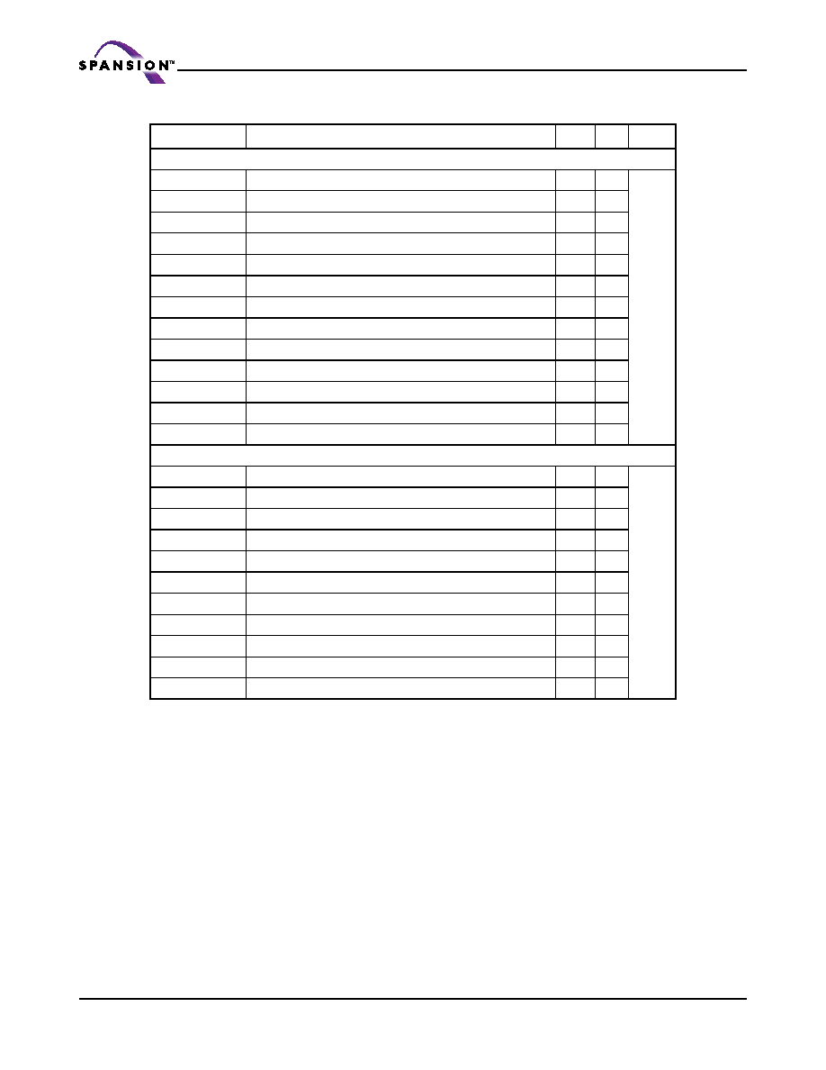
Table 26. Switching Characteristics
Notes:
1. Test conditions assume signal transition time of 1V/ns or higher, timing reference levels of VCC(typ.) /2, input pulse levels of
0 to VCC(typ.), and output loading of the specified IOL/IOH and 30 pF load capacitance.
2. tHZOE, tHZCE, tHZBE and tHZWE transitions are measured when the outputs enter a high-impedance state.
3. High-Z and Low-Z parameters are characterized and are not 100% tested.
4. To achieve 55-ns performance, the read access should be CE# controlled. In this case tACE is the critical parameter and tSK is
satisfied when the addresses are stable prior to chip enable going active. For the 70-ns cycle, the addresses must be stable
within 10 ns after the start of the read cycle.
5. The internal write time of the memory is defined by the overlap of WE#, CE#1 = VIL, CE2 = VIH, BHE and/or BLE =VIL. All
signals must be Active to initiate a write and any of these signals can terminate a write by going Inactive. The data input set-
up and hold timing should be referenced to the edge of the signal that terminates write.
Parameter
Description
Min
Max
Unit
Read Cycle
tRC
Read Cycle Time
70
ns
tAA
Address to Data Valid
70
tOHA
Data Hold from Address Change
10
tACE
CE#1 Low and CE2 High to Data Valid
70
tDOE
OE# Low to Data Valid
35
tLZOE
OE# Low to Low Z (note 2, 3)
5
tHZOE
OE# High to High Z (note 2, 3)
25
tLZCE
CE#1 Low and CE2 High to Low Z (note 2, 3)
5
tHZCE
CE#1 High and CE2 Low to High Z (note 2, 3)
25
tDBE
BHE# / BLE# Low to Data Valid
70
tLZBE
BHE# / BLE# Low to Low Z (note 2, 3)
5
tHZBE
BHE# / BLE# High to High Z (note 2, 3)
25
tSK (note 4)
Address Skew
10
Write Cycle (note 5)
tWC
Write Cycle Time
70
ns
tSCE
CE#1 Low an CE2 High to Write End
55
tAW
Address Set-Up to Write End
55
tHA
Address Hold from Write End
0
tSA
Address Set-Up to Write Start
0
tPWE
WE# Pulse Width
55
tBW
BLE# / BHE# LOW to Write End
55
tSD
Data Set-up to Write End
25
tHD
Data Hold from Write End
0
tHZWE
WE# Low to High Z (note 2, 3)
25
tLZWE
WE# High to Low Z (note 2, 3)
5
相关PDF资料 |
PDF描述 |
|---|---|
| S71GL064A04BFI0B2 | Stacked Multi-Chip Product (MCP) Flash Memory and RAM |
| S71GL064A04BFI0B3 | Stacked Multi-Chip Product (MCP) Flash Memory and RAM |
| S71GL064A04BFI0F3 | Stacked Multi-Chip Product (MCP) Flash Memory and RAM |
| S71GL064A04BFI0F2 | Stacked Multi-Chip Product (MCP) Flash Memory and RAM |
| S71GL064A04BFW0B2 | Stacked Multi-Chip Product (MCP) Flash Memory and RAM |
相关代理商/技术参数 |
参数描述 |
|---|---|
| S71GL064A04BFI0B0 | 制造商:SPANSION 制造商全称:SPANSION 功能描述:Stacked Multi-Chip Product (MCP) Flash Memory and RAM |
| S71GL064A04BFI0B2 | 制造商:SPANSION 制造商全称:SPANSION 功能描述:Stacked Multi-Chip Product (MCP) Flash Memory and RAM |
| S71GL064A04BFI0B3 | 制造商:SPANSION 制造商全称:SPANSION 功能描述:Stacked Multi-Chip Product (MCP) Flash Memory and RAM |
| S71GL064A04BFI0F0 | 制造商:SPANSION 制造商全称:SPANSION 功能描述:Stacked Multi-Chip Product (MCP) Flash Memory and RAM |
| S71GL064A04BFI0F2 | 制造商:SPANSION 制造商全称:SPANSION 功能描述:Stacked Multi-Chip Product (MCP) Flash Memory and RAM |
发布紧急采购,3分钟左右您将得到回复。