- 您现在的位置:买卖IC网 > PDF目录25644 > SI5338N-AXXXXXGM (SILICON LABORATORIES) 700 MHz, PROC SPECIFIC CLOCK GENERATOR, QCC24 PDF资料下载
参数资料
| 型号: | SI5338N-AXXXXXGM |
| 厂商: | SILICON LABORATORIES |
| 元件分类: | 时钟产生/分配 |
| 英文描述: | 700 MHz, PROC SPECIFIC CLOCK GENERATOR, QCC24 |
| 封装: | 4 X 4 MM, ROHS COMPLIANT, MO-220VGGD-8, QFN-24 |
| 文件页数: | 27/42页 |
| 文件大小: | 380K |
| 代理商: | SI5338N-AXXXXXGM |
第1页第2页第3页第4页第5页第6页第7页第8页第9页第10页第11页第12页第13页第14页第15页第16页第17页第18页第19页第20页第21页第22页第23页第24页第25页第26页当前第27页第28页第29页第30页第31页第32页第33页第34页第35页第36页第37页第38页第39页第40页第41页第42页
Si5338
Rev. 1.0
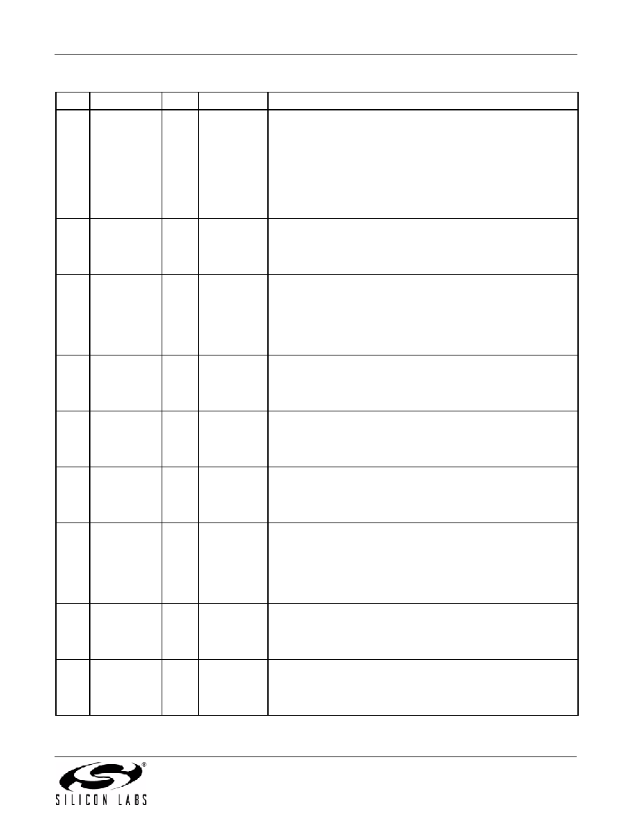
33
5,6
IN5/IN6
I
Multi
FDBK/FDBKB.
These pins can be used as a differential feedback input in zero
delay mode or as a secondary clock input. See section 3.2,
Figure 3, for termination details. See "3.10.6. Zero-Delay Mode" on
page 26 for zero delay mode set-up. Inputs to these pins must be
ac-coupled.
When not in use, leave IN5 unconnected and IN6 connected to
GND.
7
VDD
Supply
Core Supply Voltage.
This is the core supply voltage, which can operate from a 1.8, 2.5,
or 3.3 V supply. A 0.1 F bypass capacitor should be located very
close to this pin.
8
INTR
O
Open Drain
Interrupt.
A typical pullup resistor of 1–4 k
is used on this pin. This pin can
be pulled up to a supply voltage as high as 3.6 V regardless of the
other supply voltages on pins 7, 11, 15, 16, 20, and 24. The inter-
rupt condition allows the pull up resistor to pull the output up to the
supply voltage.
9
CLK3B
O
Multi
Output Clock B for Channel 3.
May be a single-ended output or half of a differential output with
CLK3A being the other differential half. If unused, leave this pin
floating.
10
CLK3A
O
Multi
Output Clock A for Channel 3.
May be a single-ended output or half of a differential output with
CLK3B being the other differential half. If unused, leave this pin
floating.
11
VDDO3
VDD
Supply
Output Clock Supply Voltage.
Supply voltage (3.3, 2.5, 1.8, or 1.5 V) for CLK3A,B. A 0.1 F
capacitor must be located very close to this pin. If CLK3 is not
used, this pin must be tied to VDD (pin 7, 24).
12
SCL
I
LVCMOS
I2C Serial Clock Input.
This is the serial clock input for the I2C bus. A pullup resistor at this
pin is required. Typical values would be 1–4 k
. See the I2C bus
spec for more information. This pin is 3.3 V tolerant regardless of
the other supply voltages on pins 7, 11, 15, 16, 20, 24. See Regis-
ter 27.
13
CLK2B
O
Multi
Output Clock B for Channel 2.
May be a single-ended output or half of a differential output with
CLK2A being the other differential half. If unused, leave this pin
floating.
14
CLK2A
O
Multi
Output Clock A for Channel 2.
May be a single-ended output or half of a differential output with
CLK2B being the other differential half. If unused, leave this pin
floating.
Table 15. Si5338 Pin Descriptions (Continued)
Pin #
Pin Name
I/O
Signal Type
Description
相关PDF资料 |
PDF描述 |
|---|---|
| SL28540ALCT | OTHER CLOCK GENERATOR, QCC56 |
| SL5504 | 1 CHANNEL TRANSISTOR OUTPUT OPTOCOUPLER |
| SL5582.3S | 1 CHANNEL TRANSISTOR OUTPUT OPTOCOUPLER |
| SLA-360MTT32S | T-1 SINGLE COLOR LED, YELLOW GREEN, 3.1 mm |
| SLA-570LT3FXH | T-1 3/4 SINGLE COLOR LED, RED, 5 mm |
相关代理商/技术参数 |
参数描述 |
|---|---|
| SI5338N-B01504-GM | 制造商:Silicon Laboratories Inc 功能描述:CLOCK - Bulk |
| SI5338N-B01504-GMR | 制造商:Silicon Laboratories Inc 功能描述:CLOCK - Tape and Reel |
| SI5338N-B01552-GM | 制造商:Silicon Laboratories Inc 功能描述:CLOCK - Bulk |
| SI5338N-B01552-GMR | 制造商:Silicon Laboratories Inc 功能描述:CLOCK - Tape and Reel |
| SI5338N-B01598-GM | 制造商:Silicon Laboratories Inc 功能描述:CLOCK - Bulk |
发布紧急采购,3分钟左右您将得到回复。