- 您现在的位置:买卖IC网 > PDF目录25644 > SI5338N-AXXXXXGM (SILICON LABORATORIES) 700 MHz, PROC SPECIFIC CLOCK GENERATOR, QCC24 PDF资料下载
参数资料
| 型号: | SI5338N-AXXXXXGM |
| 厂商: | SILICON LABORATORIES |
| 元件分类: | 时钟产生/分配 |
| 英文描述: | 700 MHz, PROC SPECIFIC CLOCK GENERATOR, QCC24 |
| 封装: | 4 X 4 MM, ROHS COMPLIANT, MO-220VGGD-8, QFN-24 |
| 文件页数: | 28/42页 |
| 文件大小: | 380K |
| 代理商: | SI5338N-AXXXXXGM |
第1页第2页第3页第4页第5页第6页第7页第8页第9页第10页第11页第12页第13页第14页第15页第16页第17页第18页第19页第20页第21页第22页第23页第24页第25页第26页第27页当前第28页第29页第30页第31页第32页第33页第34页第35页第36页第37页第38页第39页第40页第41页第42页
Si5338
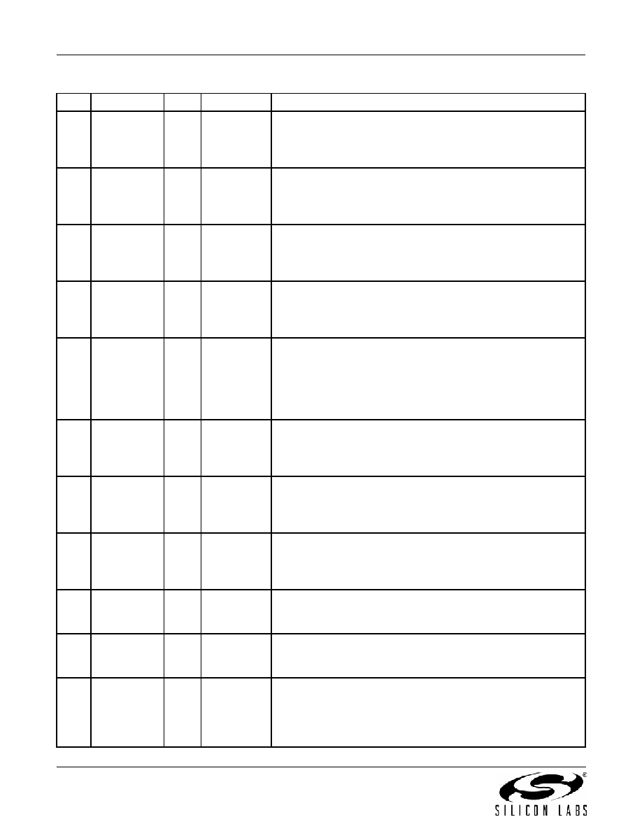
34
Rev. 1.0
15
VDDO2
VDD
Supply
Output Clock Supply Voltage.
Supply voltage (3.3, 2.5, 1.8, or 1.5 V) for CLK2A,B.
A 0.1 F capacitor must be located very close to this pin. If CLK2 is
not used, this pin must be tied to VDD (pin 7, 24).
16
VDDO1
VDD
Supply
Output Clock Supply Voltage.
Supply voltage (3.3, 2.5, 1.8, or 1.5 V) for CLK1A,B.
A 0.1 F capacitor must be located very close to this pin. If CLK1 is
not used, this pin must be tied to VDD (pin 7, 24).
17
CLK1B
O
Multi
Output Clock B for Channel 1.
May be a single-ended output or half of a differential output with
CLK1A being the other differential half. If unused, leave this pin
floating.
18
CLK1A
O
Multi
Output Clock A for Channel 1.
May be a single-ended output or half of a differential output with
CLK1B being the other differential half. If unused, leave this pin
floating.
19
SDA
I/O
LVCMOS
I2C Serial Data.
This is the serial data for the I2C bus. A pullup resistor at this pin is
required. Typical values would be 1–4 k
. See the I2C bus spec
for more information. This pin is 3.3 V tolerant regardless of the
other supply voltages on pins 7, 11, 15, 16, 20, 24. See Register
27.
20
VDDO0
VDD
Supply
Output Clock Supply Voltage.
Supply voltage (3.3, 2.5, 1.8, or 1.5 V) for CLK0A,B.
A 0.1 F capacitor must be located very close to this pin. If CLK0 is
not used, this pin must be tied to VDD (pin 7, 24).
21
CLK0B
O
Multi
Output Clock B for Channel 0.
May be a single-ended output or half of a differential output with
CLK0A being the other differential half. If unused, leave this pin
floating.
22
CLK0A
O
Multi
Output Clock A for Channel 0.
May be a single-ended output or half of a differential output with
CLK0B being the other differential half. If unused, leave this pin
floating.
23
RSVD_GND
GND
Ground.
Must be connected to system ground. Minimize the ground path
impedance for optimal performance of this device.
24
VDD
Supply
Core Supply Voltage.
The device operates from a 1.8, 2.5, or 3.3 V supply. A 0.1 F
bypass capacitor should be located very close to this pin.
GND
PAD
GND
Ground Pad.
This is the large pad in the center of the package. Device
specifications cannot be guaranteed unless the ground pad is
properly connected to a ground plane on the PCB. See Table 18,
“PCB Land Pattern,” on page 38 for ground via requirements.
Table 15. Si5338 Pin Descriptions (Continued)
Pin #
Pin Name
I/O
Signal Type
Description
相关PDF资料 |
PDF描述 |
|---|---|
| SL28540ALCT | OTHER CLOCK GENERATOR, QCC56 |
| SL5504 | 1 CHANNEL TRANSISTOR OUTPUT OPTOCOUPLER |
| SL5582.3S | 1 CHANNEL TRANSISTOR OUTPUT OPTOCOUPLER |
| SLA-360MTT32S | T-1 SINGLE COLOR LED, YELLOW GREEN, 3.1 mm |
| SLA-570LT3FXH | T-1 3/4 SINGLE COLOR LED, RED, 5 mm |
相关代理商/技术参数 |
参数描述 |
|---|---|
| SI5338N-B01504-GM | 制造商:Silicon Laboratories Inc 功能描述:CLOCK - Bulk |
| SI5338N-B01504-GMR | 制造商:Silicon Laboratories Inc 功能描述:CLOCK - Tape and Reel |
| SI5338N-B01552-GM | 制造商:Silicon Laboratories Inc 功能描述:CLOCK - Bulk |
| SI5338N-B01552-GMR | 制造商:Silicon Laboratories Inc 功能描述:CLOCK - Tape and Reel |
| SI5338N-B01598-GM | 制造商:Silicon Laboratories Inc 功能描述:CLOCK - Bulk |
发布紧急采购,3分钟左右您将得到回复。