- 您现在的位置:买卖IC网 > PDF目录25644 > SI5338N-AXXXXXGM (SILICON LABORATORIES) 700 MHz, PROC SPECIFIC CLOCK GENERATOR, QCC24 PDF资料下载
参数资料
| 型号: | SI5338N-AXXXXXGM |
| 厂商: | SILICON LABORATORIES |
| 元件分类: | 时钟产生/分配 |
| 英文描述: | 700 MHz, PROC SPECIFIC CLOCK GENERATOR, QCC24 |
| 封装: | 4 X 4 MM, ROHS COMPLIANT, MO-220VGGD-8, QFN-24 |
| 文件页数: | 4/42页 |
| 文件大小: | 380K |
| 代理商: | SI5338N-AXXXXXGM |
第1页第2页第3页当前第4页第5页第6页第7页第8页第9页第10页第11页第12页第13页第14页第15页第16页第17页第18页第19页第20页第21页第22页第23页第24页第25页第26页第27页第28页第29页第30页第31页第32页第33页第34页第35页第36页第37页第38页第39页第40页第41页第42页
Si5338
12
Rev. 1.0
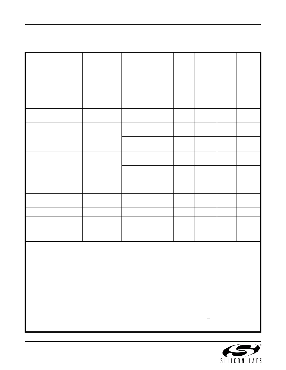
Table 12. Jitter Specifications1,2,3
(VDD = 1.8 V –5% to +10%, 2.5 V ±10%, or 3.3 V ±10%, TA = –40 to 85 °C)
Parameter
Symbol
Test Condition
Min
Typ
Max
Unit
GbE Random Jitter
(12kHz–20MHz)4
JGbE
CLKIN = 25 MHz
All CLKn at 125 MHz5
—
0.7
1
ps RMS
GbE Random Jitter
(1.875–20 MHz)
RJGbE
CLKIN = 25 MHz
All CLKn at 125 MHz5
—
0.38
0.79
ps RMS
OC-12 Random Jitter
(12 kHz–5 MHz)
JOC12
CLKIN = 19.44 MHz
All CLKn at
155.52 MHz5
—
0.7
1
ps RMS
PCI Express 1.1 Common
Clocked
Total Jitter6
—
11.2
33.6
ps pk-pk
PCI Express 2.1 Common
Clocked
RMS Jitter6, 10 kHz to
1.5 MHz
—
0.49
1.47
ps RMS
RMS Jitter6, 1.5 MHz to
50 MHz
—
0.25
0.75
ps RMS
PCI Express 2.1 Data
Clocked
RMS Jitter6, 10 kHz to
1.5 MHz
—
0.65
1.95
ps RMS
RMS Jitter6, 1.5 MHz to
50 MHz
—
0.79
2.37
ps RMS
PCI Express 3.0 Common
Clocked
RMS Jitter6
—
0.15
0.45
ps RMS
PCI Express 3.0 Data
Clocked
RMS Jitter6
—
0.17
0.51
ps RMS
Period Jitter
JPER
N = 10,000 cycles7
—
10
30
ps pk-pk
Cycle-Cycle Jitter
JCC
N = 10,000 cycles
Output MultiSynth
operated in integer or
fractional mode7
—
9
29
ps pk8
Notes:
1. All jitter measurements apply for LVDS/HCSL/LVPECL output format with a low noise differential input clock and are
made with an Agilent 90804 oscilloscope. All RJ measurements use RJ/DJ separation.
2. For best jitter performance, keep the single ended clock input slew rates at Pins 3 and 4 more than 1.0 V/ns and the
differential clock input slew rates more than 0.3 V/ns.
3. All jitter data in this table is based upon all output formats being differential. When single-ended outputs are used, there
is the potential that the output jitter may increase due to the nature of single-ended outputs. If your configuration
implements any single-ended output and any output is required to have jitter less than 3 ps rms, contact Silicon Labs
for support to validate your configuration and ensure the best jitter performance. In many configurations, CMOS
outputs have little to no effect upon jitter.
4. DJ for PCI and GbE is < 5 ps pp
5. Output MultiSynth in Integer mode.
6. All output clocks 100 MHz HCSL format. Jitter is from the PCIE jitter filter combination that produces the highest jitter.
See AN562 for details.
7. Input frequency to the Phase Detector between 25 and 40 MHz and any output frequency > 5MHz.
8. Measured in accordance with JEDEC standard 65.
9. Rj is multiplied by 14; estimate the pp jitter from Rj over 212 rising edges.
相关PDF资料 |
PDF描述 |
|---|---|
| SL28540ALCT | OTHER CLOCK GENERATOR, QCC56 |
| SL5504 | 1 CHANNEL TRANSISTOR OUTPUT OPTOCOUPLER |
| SL5582.3S | 1 CHANNEL TRANSISTOR OUTPUT OPTOCOUPLER |
| SLA-360MTT32S | T-1 SINGLE COLOR LED, YELLOW GREEN, 3.1 mm |
| SLA-570LT3FXH | T-1 3/4 SINGLE COLOR LED, RED, 5 mm |
相关代理商/技术参数 |
参数描述 |
|---|---|
| SI5338N-B01504-GM | 制造商:Silicon Laboratories Inc 功能描述:CLOCK - Bulk |
| SI5338N-B01504-GMR | 制造商:Silicon Laboratories Inc 功能描述:CLOCK - Tape and Reel |
| SI5338N-B01552-GM | 制造商:Silicon Laboratories Inc 功能描述:CLOCK - Bulk |
| SI5338N-B01552-GMR | 制造商:Silicon Laboratories Inc 功能描述:CLOCK - Tape and Reel |
| SI5338N-B01598-GM | 制造商:Silicon Laboratories Inc 功能描述:CLOCK - Bulk |
发布紧急采购,3分钟左右您将得到回复。