- 您现在的位置:买卖IC网 > Datasheet目录514 > SI8417DB-T2-E1 (Vishay Siliconix)MOSFET P-CH 12V 14.5A 2X2 6MFP Datasheet资料下载
参数资料
| 型号: | SI8417DB-T2-E1 |
| 厂商: | Vishay Siliconix |
| 文件页数: | 9/11页 |
| 文件大小: | 0K |
| 描述: | MOSFET P-CH 12V 14.5A 2X2 6MFP |
| 标准包装: | 3,000 |
| 系列: | TrenchFET® |
| FET 型: | MOSFET P 通道,金属氧化物 |
| FET 特点: | 逻辑电平门 |
| 漏极至源极电压(Vdss): | 12V |
| 电流 - 连续漏极(Id) @ 25° C: | 14.5A |
| 开态Rds(最大)@ Id, Vgs @ 25° C: | 21 毫欧 @ 1A,4.5V |
| Id 时的 Vgs(th)(最大): | 900mV @ 250µA |
| 闸电荷(Qg) @ Vgs: | 57nC @ 5V |
| 输入电容 (Ciss) @ Vds: | 2220pF @ 6V |
| 功率 - 最大: | 6.57W |
| 安装类型: | 表面贴装 |
| 封装/外壳: | 6-MICRO FOOT? |
| 供应商设备封装: | 6-Micro Foot? |
| 包装: | 带卷 (TR) |
�� �
�
�AN824�
�Vishay� Siliconix�
�TABLE� 1�
�Main� Parameters� of� Solder� Bumps� in� MICRO� FOOT� Designs�
�MICRO� FOOT� CSP�
�MICRO� FOOT� CSP� MOSFET�
�MICRO� FOOT� CSP� Analog� Switch�
�MICRO� FOOT� UCSP� Analog� Switch�
�Bump� Material�
�Eutectic� Solder:�
�63Sm/37Pb�
�Bump� Pitch*�
�0.8�
�0.5�
�0.5�
�Bump� Diameter*�
�0.37-0.41�
�0.18-0.25�
�0.32-0.34�
�Bump� Height*�
�0.26-0.29�
�0.14-0.19�
�0.21-0.24�
�*� All� measurements� in� millimeters�
�MICRO� FOOT’S� DESIGN� AND� RELIABILITY�
�As� a� mechanical,� electrical,� and� thermal� connection� between�
�the� device� and� PCB,� the� solder� bumps� of� MICRO� FOOT�
�products� are� mounted� on� the� top� active� surface� of� the� die.�
�Table� 1� shows� the� main� parameters� for� solder� bumps� used� in�
�MICRO� FOOT� products.� A� silicon� nitride� passivation� layer� is�
�applied� to� the� active� area� as� the� last� masking� process� in�
�fabrication,ensuring� that� the� device� passes� the� pressure� pot�
�test.� A� green� laser� is� used� to� mark� the� backside� of� the� die�
�without� damaging� it.� Reliability� results� for� MICRO� FOOT�
�products� mounted� on� a� FR-4� board� without� underfill� are� shown�
�in� Table� 2.�
�TABLE� 2�
�MICRO� FOOT� Reliability� Results�
�Test� Condition� C:� ?� 65� _� to� 150� _� C� >500� Cycles�
�Test� condition� B:� ?� 40� _� to� 125� _� C� >1000� Cycles�
�121� _� C� @� 15PSI� 100%� Humidity� Test� 96� Hours�
�The� main� failure� mechanism� associated� with� wafer-level�
�chip-scale� packaging� is� fatigue� of� the� solder� joint.� The� results�
�shown� in� Table� 2� demonstrate� that� a� high� level� of� reliability� can�
�be� achieved� with� proper� board� design� and� assembly�
�techniques.�
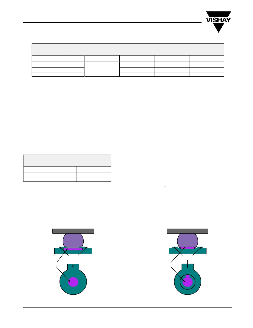
�Solder� Mask�
�Copper�
�FIGURE� 3.� SMD�
�www.vishay.com�
�2�
�BOARD� LAYOUT� GUIDELINES�
�Board� materials� .� Vishay� Siliconix� MICRO� FOOT� products� are�
�designed� to� be� reliable� on� most� board� types,� including� organic�
�boards� such� as� FR-4� or� polyamide� boards.� The� package�
�qualification� information� is� based� on� the� test� on� 0.5-oz.� FR-4�
�and� polyamide� boards� with� NSMD� pad� design.�
�Land� patterns.� Two� types� of� land� patterns� are� used� for�
�surface-mount� packages.� Solder� mask� defined� (SMD)� pads�
�have� a� solder� mask� opening� smaller� than� the� metal� pad�
�(Figure� 3),� whereas� on-solder� mask� defined� (NSMD)� pads�
�have� a� metal� pad� smaller� than� the� solder-mask� opening�
�(Figure� 4).�
�NSMD� is� recommended� for� copper� etch� processes,� since� it�
�provides� a� higher� level� of� control� compared� to� SMD� etch�
�processes.� A� small-size� NSMD� pad� definition� provides� more�
�area� (both� lateral� and� vertical)� for� soldering� and� more� room� for�
�escape� routing� on� the� PCB.� By� contrast,� SMD� pad� definition�
�introduces� a� stress� concentration� point� near� the� solder� mask�
�on� the� PCB� side� that� may� result� in� solder� joint� cracking� under�
�extreme� fatigue� conditions.�
�Copper� pads� should� be� finished� with� an� organic� solderability�
�preservative� (OSP)� coating.� For� electroplated�
�nickel-immersion� gold� finish� pads,� the� gold� thickness� must� be�
�less� than� 0.5� m� m� to� avoid� solder� joint� embrittlement.�
�Solder� Mask�
�Copper�
�FIGURE� 4.� NSMD�
�Document� Number:� 71990�
�06-Jan-03�
�相关PDF资料 |
PDF描述 |
|---|---|
| SI8439DB-T1-E1 | MOSFET P-CH 8V D-S MICROFOOT |
| SI8441DB-T2-E1 | MOSFET P-CH 20V 10.5A 2X2 6MFP |
| SI8447DB-T2-E1 | MOSFET P-CH D-S 20V MICROFOOT |
| SI8461DB-T2-E1 | MOSFET P-CH D-S 20V MICROFOOT |
| SI8465DB-T2-E1 | MOSFET P-CH D-S 20V MICROFOOT |
相关代理商/技术参数 |
参数描述 |
|---|---|
| SI84-180 | 制造商:DELTA 制造商全称:Delta Electronics, Inc. 功能描述:SMT Power Inductor |
| SI84-180K | 制造商:DELTA 制造商全称:Delta Electronics, Inc. 功能描述:SMT Power Inductor |
| SI84-181 | 制造商:DELTA 制造商全称:Delta Electronics, Inc. 功能描述:SMT Power Inductor |
| SI84-181K | 制造商:DELTA 制造商全称:Delta Electronics, Inc. 功能描述:SMT Power Inductor |
| SI8419DB-T1-E1 | 功能描述:MOSFET 8.0V 11.7A 6.25W 35mohm @ 4.5V RoHS:否 制造商:STMicroelectronics 晶体管极性:N-Channel 汲极/源极击穿电压:650 V 闸/源击穿电压:25 V 漏极连续电流:130 A 电阻汲极/源极 RDS(导通):0.014 Ohms 配置:Single 最大工作温度: 安装风格:Through Hole 封装 / 箱体:Max247 封装:Tube |
发布紧急采购,3分钟左右您将得到回复。