- 您现在的位置:买卖IC网 > PDF目录98083 > SME1430LGA-480 64-BIT, 480 MHz, RISC PROCESSOR, CBGA587 PDF资料下载
参数资料
| 型号: | SME1430LGA-480 |
| 元件分类: | 微控制器/微处理器 |
| 英文描述: | 64-BIT, 480 MHz, RISC PROCESSOR, CBGA587 |
| 封装: | CERAMIC, LGA-587 |
| 文件页数: | 14/60页 |
| 文件大小: | 646K |
| 代理商: | SME1430LGA-480 |
第1页第2页第3页第4页第5页第6页第7页第8页第9页第10页第11页第12页第13页当前第14页第15页第16页第17页第18页第19页第20页第21页第22页第23页第24页第25页第26页第27页第28页第29页第30页第31页第32页第33页第34页第35页第36页第37页第38页第39页第40页第41页第42页第43页第44页第45页第46页第47页第48页第49页第50页第51页第52页第53页第54页第55页第56页第57页第58页第59页第60页
21
Highly Integrated 64-Bit RISC; L2-Cache, DRAM, PCI Interfaces
UltraSPARC-IIi CPU
SME1430LGA-360
SME1430LGA-440
SME1430LGA-480
May 1999
Sun Microsystems, Inc
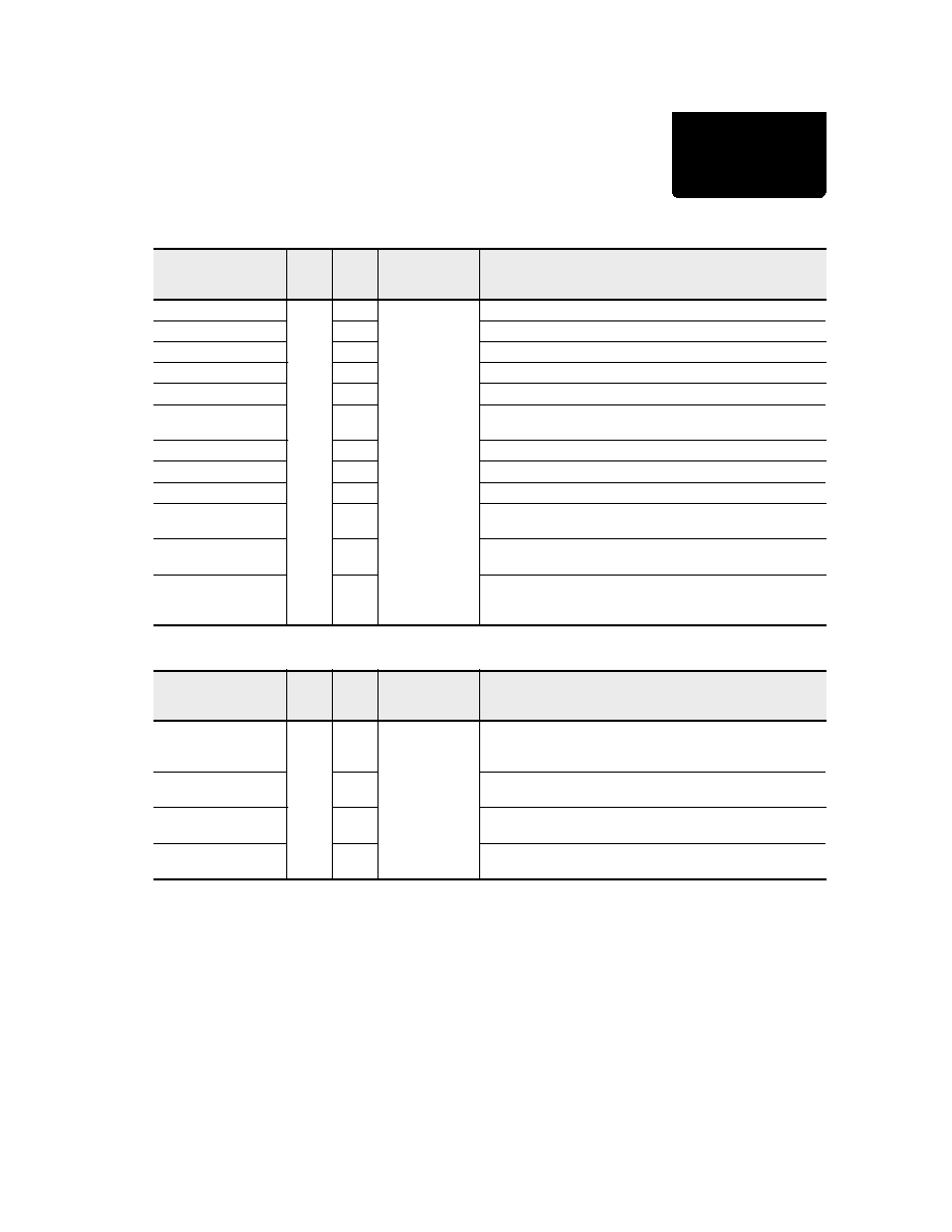
Memory and Transceiver Interface
Symbol
Volts
Type
Signal
Transitions
Aligned with:
Name and Function
MEM_WE_L
3.3 V
(All)
O
CLKA/B
Memory Write Enable; active low
MEM_CAS_L[1:0]
O
Memory Column Address Strobe; active low
MEM_RAST_L{3:0]
O
Memory Row Address Strobe Top; active low
MEM_RASB_L[3:0]
O
Memory Row Address Strobe Bottom, active low
MEM_DATA[71:0]
I/O
Memory Data; bits [71:64] are ECC bits
MEM_ADDR[12:0]
O
Memory Address, row and column (10 and 11 bit column
support)
XCVR_OEA_L
O
Transceiver Output Enable A; active low
XCVR_OEB_L
O
Transceiver Output Enable B; active low
XCVR_SEL_L
O
Transceiver Select; active low; picks high or low half of read data
XCVR_WR_CNTL[1:0]
O
Transceiver Write Control; controls lock enables on internal
registers
XCVR_RD_CNTL[1:0]
O
Transceiver Read Control; control clock enables on internal
registers
XCVR_CLK[2:0]
O
Transceiver Clock; all data and control signals are registered by
these clocks; multiple outputs to minimize loading effects of 6
transceivers
UPA64S Interface
Symbol
Volts
Type
Signal
Transitions
Aligned with:
Name and Function
S_REPLY[2:0]
3.3 V
O
UPA_CLK_POS/
UPA_CLK_NEG
S Reply; encoded command indicates arrival of write data on
MEM_DATA[63:0], or command to drive MEM_DATA[63:0] with
read data
P_REPLY[1:0]
I
P Reply; encoded command that indicates ability consumption of
prior write, or ability to provide read data
SYSADR[28:0]
I/O [1]
1. Not all of SYSADR[28:0] is bidirectional, since SYSADR[14:0] is I/O but SYSADR[28:15] is output only. SYSADR[14:0] is used as an input during
RAM_TEST.
System Address; sends 2 cycle address packet to UPA64S slave,
or provides internal state debug information
ADR_VLD
O
Address Valid; asserted during rst cycle of two cycle address
packet
相关PDF资料 |
PDF描述 |
|---|---|
| SME1701-BGA133 | 32-BIT, 133 MHz, MICROPROCESSOR, PBGA316 |
| SME5224AUPA-360 | 64-BIT, 360 MHz, RISC PROCESSOR |
| SME5410MCZ-270 | 64-BIT, 270 MHz, RISC PROCESSOR, XMA |
| SME5434PCI-440 | 64-BIT, 440 MHz, RISC PROCESSOR, XMA |
| SME5434PCI-480 | 64-BIT, 480 MHz, RISC PROCESSOR, XMA |
相关代理商/技术参数 |
参数描述 |
|---|---|
| SME14P95J4173 | 制造商:LIT 功能描述:Connector |
| SME160T1R0H | 制造商:Russell 功能描述: |
| SME160T221M22X40LL | 制造商:United Chemi-Con Inc 功能描述: |
| SME160T2R2H | 制造商:Russell 功能描述: |
| SME160VB10RM10X16FT | 制造商:United Chemi-Con Inc 功能描述: |
发布紧急采购,3分钟左右您将得到回复。