- 您现在的位置:买卖IC网 > PDF目录98083 > SME1430LGA-480 64-BIT, 480 MHz, RISC PROCESSOR, CBGA587 PDF资料下载
参数资料
| 型号: | SME1430LGA-480 |
| 元件分类: | 微控制器/微处理器 |
| 英文描述: | 64-BIT, 480 MHz, RISC PROCESSOR, CBGA587 |
| 封装: | CERAMIC, LGA-587 |
| 文件页数: | 9/60页 |
| 文件大小: | 646K |
| 代理商: | SME1430LGA-480 |
第1页第2页第3页第4页第5页第6页第7页第8页当前第9页第10页第11页第12页第13页第14页第15页第16页第17页第18页第19页第20页第21页第22页第23页第24页第25页第26页第27页第28页第29页第30页第31页第32页第33页第34页第35页第36页第37页第38页第39页第40页第41页第42页第43页第44页第45页第46页第47页第48页第49页第50页第51页第52页第53页第54页第55页第56页第57页第58页第59页第60页
17
Highly Integrated 64-Bit RISC; L2-Cache, DRAM, PCI Interfaces
UltraSPARC-IIi CPU
SME1430LGA-360
SME1430LGA-440
SME1430LGA-480
May 1999
Sun Microsystems, Inc
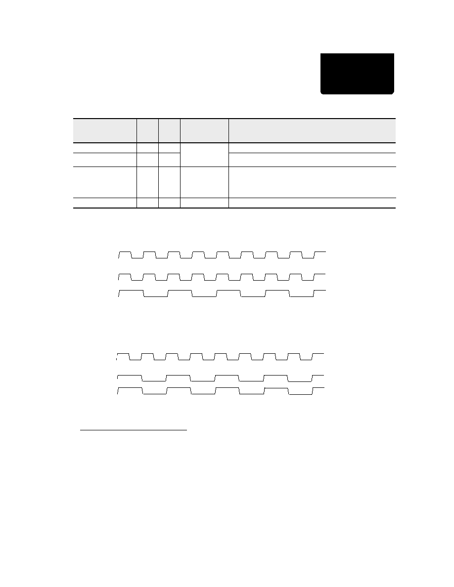
PCI Clock Timing [1] [2]
Figure 5. Relation Between PCI (1X Mode) Clocks [3]
Figure 6. Relation Between PCI (2X Mode) Clocks [4] [5]
PCI Clock Interface
Symbol
Volts
Type
Signal
Transitions
Aligned with:
Name and Function
PCI_REF_CLK
3.3 V
I
See
and
Figure 6 for
logical relations.
PCI reference clock; 40-66 MHz.
PCI_CLK
3.3 V
I
PCI clock, 66mhz; can be set to 33 MHz PCI interface if desired.
P2L5CLK
1.9 V
O
PCI_REF_CLK
Disabled during normal operation; internal level 5 clock that
reects the PCI clock and is used to determine PLL lock or clock
tree delay when in PLLBYPASS mode; during PLLBYPASS mode,
PCI_REF_CLK must be 2X frequency of PCI_CLK
PLLBYPASS
1. See Figure 28 and table: "Clock Skew" for skew requirements for PCI_REF_CLK.
2. During PLLBYPASS the PCI_CLK and PCI_REF_CLK relationships must be the same as for PCI 1X Mode.
3. Figure 5 applies to the PCI bus clock between 20-33 MHz, which must be in 1X mode.
4. Figure 6 (and 2X mode) applies when the bus is run from 40-66 MHz.
5. Refer to the table: "Clock Skew" for permissible skew between PCI_REF_CLK and PCI_CLK. It is recommended
that the system designer supplies PCI_REF_CLK directly from the PCI_CLK signal for 2X mode operation – see
Figure 6. Skew between PCI_CLK and PCI_REF_CLK must be minimized; the required setup time is:
1X Mode
Internal PCICLK
PCI_REF_CLK
PCI_CLK
40 - 66 MHz
20 - 33 MHz
PCI_REF_CLK
2X Mode
Internal PCICLK
80 - 132 MHz
40 - 66 MHz
PCI_CLK
40 - 66 MHz
t
SUeff
3ns
t
SKEW_POS
+
()
=
相关PDF资料 |
PDF描述 |
|---|---|
| SME1701-BGA133 | 32-BIT, 133 MHz, MICROPROCESSOR, PBGA316 |
| SME5224AUPA-360 | 64-BIT, 360 MHz, RISC PROCESSOR |
| SME5410MCZ-270 | 64-BIT, 270 MHz, RISC PROCESSOR, XMA |
| SME5434PCI-440 | 64-BIT, 440 MHz, RISC PROCESSOR, XMA |
| SME5434PCI-480 | 64-BIT, 480 MHz, RISC PROCESSOR, XMA |
相关代理商/技术参数 |
参数描述 |
|---|---|
| SME14P95J4173 | 制造商:LIT 功能描述:Connector |
| SME160T1R0H | 制造商:Russell 功能描述: |
| SME160T221M22X40LL | 制造商:United Chemi-Con Inc 功能描述: |
| SME160T2R2H | 制造商:Russell 功能描述: |
| SME160VB10RM10X16FT | 制造商:United Chemi-Con Inc 功能描述: |
发布紧急采购,3分钟左右您将得到回复。