- 您现在的位置:买卖IC网 > PDF目录98142 > SST85LD1001T-60-RI-LBTE IDE COMPATIBLE, FLASH MEMORY DRIVE CONTROLLER, PBGA91 PDF资料下载
参数资料
| 型号: | SST85LD1001T-60-RI-LBTE |
| 元件分类: | 存储控制器/管理单元 |
| 英文描述: | IDE COMPATIBLE, FLASH MEMORY DRIVE CONTROLLER, PBGA91 |
| 封装: | 12 X 24 MM, ROHS COMPLIANT, MO-210, LBGA-91 |
| 文件页数: | 34/36页 |
| 文件大小: | 913K |
| 代理商: | SST85LD1001T-60-RI-LBTE |
第1页第2页第3页第4页第5页第6页第7页第8页第9页第10页第11页第12页第13页第14页第15页第16页第17页第18页第19页第20页第21页第22页第23页第24页第25页第26页第27页第28页第29页第30页第31页第32页第33页当前第34页第35页第36页
2009 Silicon Storage Technology, Inc.
S71382-04-000
10/09
7
512 MByte / 1 GByte / 2 GByte NANDrive
SST85LD0512 / SST85LD1001T / SST85LD1002U
Data Sheet
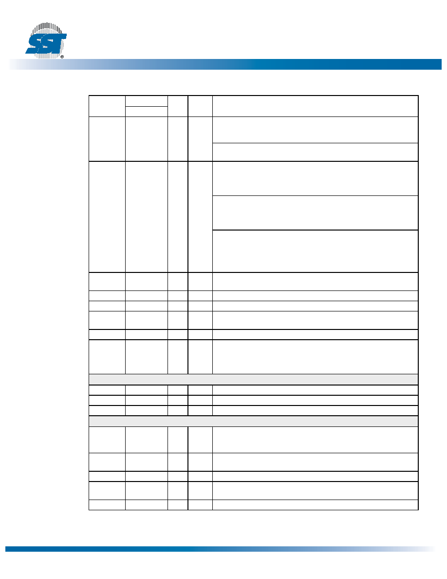
IOWR#
H9
I
I2Z
IOWR#: This is an I/O Write Strobe generated by the host. When Ultra
DMA mode is not active, this signal is used to clock I/O data into the
device.
STOP: When Ultra DMA mode protocol is active, the assertion of this
signal causes the termination of the Ultra DMA burst
IORDY
J4
O
I2Z
IORDY: When Ultra DMA mode DMA Write is not active and the
device is not ready to respond to a data transfer request, this signal is
negated to extend the Host transfer cycle. However, it is never
negated by this controller.
DDMARDY#: When Ultra DMA mode DMA Write is active, this signal
is asserted by the host to indicate that the device is ready to receive
Ultra DMA data-in bursts. The device may negate DDMARDY# to
pause an Ultra DMA transfer.
DSTROBE: When Ultra DMA mode DMA Read is active, this signal is
the data-out strobe generated by the device. Both the rising and falling
edges of DSTROBE cause data to be latched by the host. The device
may stop generating DSTROBE edges to pause an Ultra DMA data-
out burst.
IOCS16#
J8
O
O2
This output signal is asserted low when the device is indicating a word
data transfer cycle.
INTRQ
J2
O
O1
This signal is the active high Interrupt Request to the host.
PDIAG#
K9
I/O
I1U/O1 The Pass Diagnostic signal in the Master/Slave handshake protocol.
DASP#
D9
I/O
I1U/O6 The Drive Active/Slave Present signal in the Master/Slave handshake
protocol.
RESET#
E4
I
I2U
This input pin is the active low hardware reset from the host.
WP#/PD#
F6
I
I3U
The WP#/PD# pin can be used for either the Write Protect mode or
Power-down mode, but only one mode is active at any time. The Write
Protect or Power-down modes can be selected through the host com-
mand. The Write Protect mode is the factory default setting.
Serial Communication Interface (SCI)
SCIDOUT
D8
O
O4
SCI interface data output
SCIDIN
D7
I
I3U
SCI interface data input
SCICLK
E7
I
I3U
SCI interface clock
Miscellaneous
VSS
G4, G6, G7,
K4, K6, K7,
J9
PWR
Ground
VDD
E9, K5,
L5, M2
PWR
VDD (3.3V)
VDDQ
E2, M9
PWR
VDDQ (5V/3.3V) for Host interface
POR#
J7
I
Analog
Input1
Power-on Reset (POR). Active Low
VREG
D2
O
External capacitor pin
Table 1: Pin Assignments (Continued) (2 of 3)
Symbol
Pin No.
Pin
Type
I/O
Type
Name and Functions
91-TFBGA
相关PDF资料 |
PDF描述 |
|---|---|
| SST85LD1004T-60-RI-LBTE | IDE COMPATIBLE, FLASH MEMORY DRIVE CONTROLLER, PBGA91 |
| SST85LD1008M-60-PC-LBTE | IDE COMPATIBLE, FLASH MEMORY DRIVE CONTROLLER, PBGA91 |
| SST85LD1008M-60-PC-LBTE | IDE COMPATIBLE, FLASH MEMORY DRIVE CONTROLLER, PBGA91 |
| SST85LP1004A-M-C-LBTE | IDE COMPATIBLE, FLASH MEMORY DRIVE CONTROLLER, PBGA91 |
| SST85LP1004A-M-C-LBTE | IDE COMPATIBLE, FLASH MEMORY DRIVE CONTROLLER, PBGA91 |
相关代理商/技术参数 |
参数描述 |
|---|---|
| SST85LD1002L-60-4C-LBTE | 功能描述:闪存 2G NAND 60ns 3.3V Commercial RoHS:否 制造商:ON Semiconductor 数据总线宽度:1 bit 存储类型:Flash 存储容量:2 MB 结构:256 K x 8 定时类型: 接口类型:SPI 访问时间: 电源电压-最大:3.6 V 电源电压-最小:2.3 V 最大工作电流:15 mA 工作温度:- 40 C to + 85 C 安装风格:SMD/SMT 封装 / 箱体: 封装:Reel |
| SST85LD1002L-60-PC-LBTE | 功能描述:闪存 2GB NAND 60ns 3.3V Commercial RoHS:否 制造商:ON Semiconductor 数据总线宽度:1 bit 存储类型:Flash 存储容量:2 MB 结构:256 K x 8 定时类型: 接口类型:SPI 访问时间: 电源电压-最大:3.6 V 电源电压-最小:2.3 V 最大工作电流:15 mA 工作温度:- 40 C to + 85 C 安装风格:SMD/SMT 封装 / 箱体: 封装:Reel |
| SST85LD1002U-60-5I-LBTE | 功能描述:闪存 2G NAND 60ns 3.3V Industrial RoHS:否 制造商:ON Semiconductor 数据总线宽度:1 bit 存储类型:Flash 存储容量:2 MB 结构:256 K x 8 定时类型: 接口类型:SPI 访问时间: 电源电压-最大:3.6 V 电源电压-最小:2.3 V 最大工作电流:15 mA 工作温度:- 40 C to + 85 C 安装风格:SMD/SMT 封装 / 箱体: 封装:Reel |
| SST85LD1002U-60-RI-LBTE | 功能描述:闪存 2GB NAND 60ns 3.3V Industrial RoHS:否 制造商:ON Semiconductor 数据总线宽度:1 bit 存储类型:Flash 存储容量:2 MB 结构:256 K x 8 定时类型: 接口类型:SPI 访问时间: 电源电压-最大:3.6 V 电源电压-最小:2.3 V 最大工作电流:15 mA 工作温度:- 40 C to + 85 C 安装风格:SMD/SMT 封装 / 箱体: 封装:Reel |
| SST85LD1004M-60-4C-LBTE | 功能描述:闪存 4G NAND 60ns 3.3V Commercial RoHS:否 制造商:ON Semiconductor 数据总线宽度:1 bit 存储类型:Flash 存储容量:2 MB 结构:256 K x 8 定时类型: 接口类型:SPI 访问时间: 电源电压-最大:3.6 V 电源电压-最小:2.3 V 最大工作电流:15 mA 工作温度:- 40 C to + 85 C 安装风格:SMD/SMT 封装 / 箱体: 封装:Reel |
发布紧急采购,3分钟左右您将得到回复。