- 您现在的位置:买卖IC网 > PDF目录98144 > ST72141K2B3/XXX (STMICROELECTRONICS) 8-BIT, MROM, 8 MHz, MICROCONTROLLER, PDIP32 PDF资料下载
参数资料
| 型号: | ST72141K2B3/XXX |
| 厂商: | STMICROELECTRONICS |
| 元件分类: | 微控制器/微处理器 |
| 英文描述: | 8-BIT, MROM, 8 MHz, MICROCONTROLLER, PDIP32 |
| 封装: | 0.400 INCH, PLASTIC, SDIP-32 |
| 文件页数: | 25/133页 |
| 文件大小: | 2615K |
| 代理商: | ST72141K2B3/XXX |
第1页第2页第3页第4页第5页第6页第7页第8页第9页第10页第11页第12页第13页第14页第15页第16页第17页第18页第19页第20页第21页第22页第23页第24页当前第25页第26页第27页第28页第29页第30页第31页第32页第33页第34页第35页第36页第37页第38页第39页第40页第41页第42页第43页第44页第45页第46页第47页第48页第49页第50页第51页第52页第53页第54页第55页第56页第57页第58页第59页第60页第61页第62页第63页第64页第65页第66页第67页第68页第69页第70页第71页第72页第73页第74页第75页第76页第77页第78页第79页第80页第81页第82页第83页第84页第85页第86页第87页第88页第89页第90页第91页第92页第93页第94页第95页第96页第97页第98页第99页第100页第101页第102页第103页第104页第105页第106页第107页第108页第109页第110页第111页第112页第113页第114页第115页第116页第117页第118页第119页第120页第121页第122页第123页第124页第125页第126页第127页第128页第129页第130页第131页第132页第133页
Obsolete
Product(s)
- Obsolete
Product(s)
ST72141K2
120/133
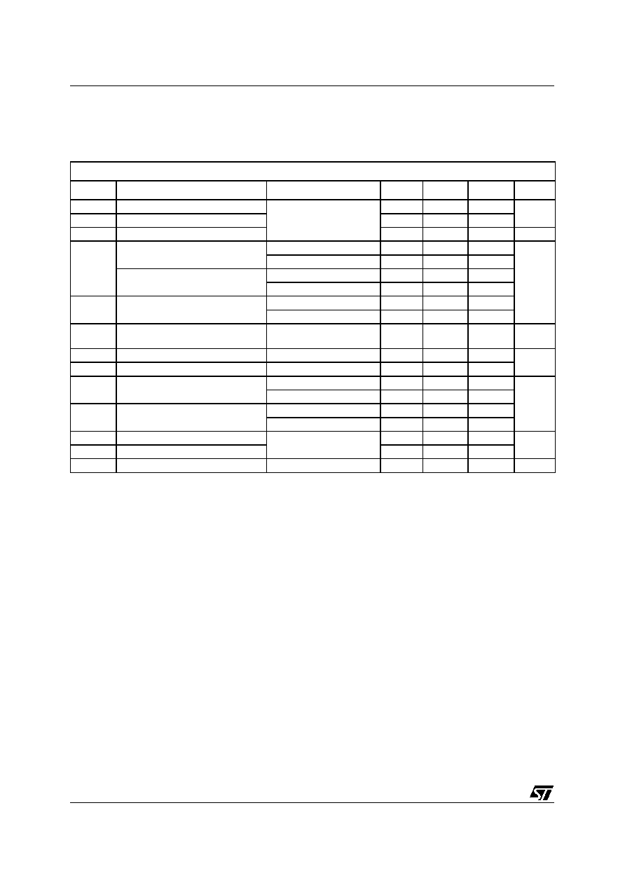
10.5 I/O PORT CHARACTERISTICS
Recommended operating conditions
with TA=-40 to +125
oC and 4.5V<V
DD-VSS<5.5V unless otherwise specified.
Notes:
1) Unless otherwise specified, typical data is based on TA=25°C and VDD-VSS=5V. This data is provided only as design
guidelines and is not tested.
2) Data based on design simulations and/or technology characteristics, not tested in production.
3) Hysteresis voltage between Schmitt trigger switching levels. Based on characterisation results, not tested.
4) Data based on characterization results, not tested in production.
5) Positive injection (IINJ+)
The IINJ+ is performed through protection diodes insulated from the substrate of the die.
The true open-drain pins do not accept positive injection. In this case the maximum voltage rating must be respected.
6) ADC accuracy reduced by negative injection (IINJ- )
The IINJ- is performed through protection diodes NOT INSULATED from the substrate of the die. The drawback is a small
leakage (a few
μA) induced inside the die when a negative injection is performed. This leakage is tolerated by the digital
structure, but it acts on the analog line depending on the impedance versus a leakage current of a few
μA (if the MCU
has an AD converter). The effect depends on the pin which is submitted to the injection. Of course, external digital signals
applied to the component must have a maximum impedance close to 50K
Ω.
Location of the negative current injection:
- Pins with analog input capability are the most sensitive. IINJ- maximum is 0.8 mA (assuming that the impedance of the
analog voltage is lower than 25K
Ω)
- Pure digital pins can tolerate 1.6mA. In addition, the best choice is to inject the current as far as possible from the analog
input pins.
7) When several inputs are submitted to a current injection, the maximum IINJ is the sum of the positive (or negative) cur-
rents (instantaneous values). These results are based on characterisation with IINJ maximum current injection on four I/
O port pins of the device.
8) To generate an external interrupt, a minimum pulse width has to be applied on an I/O port pin configured as an external
interrupt source.
I/O PORT PINS
Symbol
Parameter
Conditions
Min
Typ 1)
Max
Unit
VIL
Input low level voltage 2)
0.3xVDD
V
VIH
Input high level voltage 2)
0.7xVDD
VHYS
Schmitt trigger voltage hysteresis 3)
400
mV
VOL
Output low level voltage
for standard I/O port pins
I=-5mA
1.3
V
I=-2mA
0.5
Output low level voltage
for high sink I/O port pins
I=-20mA
1.3
I=-8mA
0.5
VOH
Output high level voltage
I=-5mA
VDD-2.0
I=-2mA
VDD-0.8
RPU
Pull-up equivalent resistor
VIN > VIH
VIN < VIL
20
50
40
120
80
240
k
Ω
IL
Input leakage current
VSS<VPIN<VDD
1
μA
ISV
Static current consumption 2)
Floating input mode
200
IPINJ
Single pin injected current
Positive 5): VEXT>VDD
5
mA
Negative 6): VEXT<VSS
-5
IINJ
Total injected current 7)
(sum of all I/O and control pins)
Positive: VEXT>VDD
20
Negative: VEXT<VSS
20
tOHL
Output high to low level fall time
Cl=50pF
14.8 4)
25
45.6 4)
ns
tOLH
Output low to high rise time
14.4 4)
25
45.9 4)
tITEXT
External interrupt pulse time 8)
1tCPU
相关PDF资料 |
PDF描述 |
|---|---|
| ST72311N4T6/XXX | 8-BIT, MROM, 8 MHz, MICROCONTROLLER, PQFP64 |
| ST72311J2B6/XXX | 8-BIT, MROM, 8 MHz, MICROCONTROLLER, PDIP42 |
| ST72311N2T3/XXX | 8-BIT, MROM, 8 MHz, MICROCONTROLLER, PQFP64 |
| ST72321BAR7T6 | MICROCONTROLLER, QFP64 |
| ST72321BR7T3 | MICROCONTROLLER, QFP64 |
相关代理商/技术参数 |
参数描述 |
|---|---|
| ST72141K2B6 | 制造商:STMICROELECTRONICS 制造商全称:STMicroelectronics 功能描述:8-BIT MCU WITH ELECTRIC-MOTOR CONTROL, ADC, 16-BIT TIMERS, SPI INTERFACE |
| ST72141K2M1 | 制造商:STMICROELECTRONICS 制造商全称:STMicroelectronics 功能描述:8-BIT MCU WITH ELECTRIC-MOTOR CONTROL, ADC, 16-BIT TIMERS, SPI INTERFACE |
| ST72141K2M3 | 制造商:STMICROELECTRONICS 制造商全称:STMicroelectronics 功能描述:8-BIT MCU WITH ELECTRIC-MOTOR CONTROL, ADC, 16-BIT TIMERS, SPI INTERFACE |
| ST72141K2M3/XXX | 制造商:未知厂家 制造商全称:未知厂家 功能描述:Microcontroller |
| ST72141K2M6 | 制造商:STMICROELECTRONICS 制造商全称:STMicroelectronics 功能描述:8-BIT MCU WITH ELECTRIC-MOTOR CONTROL, ADC, 16-BIT TIMERS, SPI INTERFACE |
发布紧急采购,3分钟左右您将得到回复。