- 您现在的位置:买卖IC网 > PDF目录69378 > ST7PL38F2MC/XXXE (STMICROELECTRONICS) 8-BIT, MROM, 8 MHz, MICROCONTROLLER, PDSO20 PDF资料下载
参数资料
| 型号: | ST7PL38F2MC/XXXE |
| 厂商: | STMICROELECTRONICS |
| 元件分类: | 微控制器/微处理器 |
| 英文描述: | 8-BIT, MROM, 8 MHz, MICROCONTROLLER, PDSO20 |
| 封装: | 0.300 INCH, ROHS COMPLIANT, PLASTIC, SOP-20 |
| 文件页数: | 86/168页 |
| 文件大小: | 2955K |
| 代理商: | ST7PL38F2MC/XXXE |
第1页第2页第3页第4页第5页第6页第7页第8页第9页第10页第11页第12页第13页第14页第15页第16页第17页第18页第19页第20页第21页第22页第23页第24页第25页第26页第27页第28页第29页第30页第31页第32页第33页第34页第35页第36页第37页第38页第39页第40页第41页第42页第43页第44页第45页第46页第47页第48页第49页第50页第51页第52页第53页第54页第55页第56页第57页第58页第59页第60页第61页第62页第63页第64页第65页第66页第67页第68页第69页第70页第71页第72页第73页第74页第75页第76页第77页第78页第79页第80页第81页第82页第83页第84页第85页当前第86页第87页第88页第89页第90页第91页第92页第93页第94页第95页第96页第97页第98页第99页第100页第101页第102页第103页第104页第105页第106页第107页第108页第109页第110页第111页第112页第113页第114页第115页第116页第117页第118页第119页第120页第121页第122页第123页第124页第125页第126页第127页第128页第129页第130页第131页第132页第133页第134页第135页第136页第137页第138页第139页第140页第141页第142页第143页第144页第145页第146页第147页第148页第149页第150页第151页第152页第153页第154页第155页第156页第157页第158页第159页第160页第161页第162页第163页第164页第165页第166页第167页第168页
Obsolete
Product(s)
- Obsolete
ST7L34, ST7L35, ST7L38, ST7L39
24/168
7 SUPPLY, RESET AND CLOCK MANAGEMENT
The device includes a range of utility features for
securing the application in critical situations (for
example in case of a power brown-out) and reduc-
ing the number of external components.
Main features
■ Clock Management
– 1 MHz internal RC oscillator (enabled by op-
tion byte)
– 1 to 16 MHz or 32 kHz External crystal/ceram-
ic resonator (selected by option byte)
– External Clock Input (enabled by option byte)
– PLL for multiplying the frequency by 8
■ Reset Sequence Manager (RSM)
■ System Integrity Management (SI)
– Main supply Low voltage detection (LVD) with
reset generation (enabled by option byte)
– Auxiliary Voltage detector (AVD) with interrupt
capability for monitoring the main supply (en-
abled by option byte)
7.1 INTERNAL RC OSCILLATOR ADJUSTMENT
The device contains an internal RC oscillator with
high accuracy for a given device, temperature and
voltage range (4.5V to 5.5V). It must be calibrated
to obtain the frequency required in the application.
This is done by software writing an 8-bit calibration
value in the RCCR (RC Control Register) and in
the bits [6:5] in the SICSR (SI Control/Status Reg-
ister).
Whenever the microcontroller is reset, the RCCR
returns to its default value (FFh), that is, each time
the device is reset, the calibration value must be
loaded in the RCCR. Predefined calibration values
are stored in EEPROM for 3V and 5V VDD supply
voltages at 25°C, as shown in the following table.
1. DEE0h, DEE1h, DEE2h and DEE3h addresses are lo-
cated in a reserved area but are special bytes containing
also the RC calibration values which are read-accessible
only in user mode. If all the EEPROM data or Flash space
(including the RC calibration values locations) has been
erased (after the readout protection removal), then the RC
calibration values can still be obtained through these four
addresses.
For compatibility reasons with the SICSR register, CR[1:0]
bits are stored in the fifth and sixth positions of DEE1 and
DEE3 addresses.
Notes:
– In ICC mode, the internal RC oscillator is forced
as a clock source, regardless of the selection in
the option byte.
page 127 for more information on the frequency
and accuracy of the RC oscillator.
– To improve clock stability and frequency accura-
cy, it is recommended to place a decoupling ca-
pacitor, typically 100nF, between the VDD and
VSS pins as close as possible to the ST7 device.
– These bytes are systematically programmed by
ST, including on FASTROM devices. Conse-
quently, customers intending to use FASTROM
service must not use these bytes.
– RCCR0 and RCCR1 calibration values will not
be erased if the readout protection bit is reset af-
ter it has been set. See “Readout Protection” on
Caution: If the voltage or temperature conditions
change in the application, the frequency might
need recalibration.
Refer to application note AN1324 for information
on how to calibrate the RC frequency using an ex-
ternal reference signal.
7.2 PHASE LOCKED LOOP
The PLL can be used to multiply a 1 MHz frequen-
cy from the RC oscillator or the external clock by 8
to obtain fOSC of 8 MHz. The PLL is enabled (by 1
option bit) and the multiplication factor is 8.
The x8 PLL is intended for operation with VDD in
the 3.6V to 5.5V range (refer to Section 15.1 for
the option byte description).
If the PLL is disabled and the RC oscillator is ena-
bled, then fOSC = 1 MHz.
If both the RC oscillator and the PLL are disabled,
fOSC is driven by the external clock.
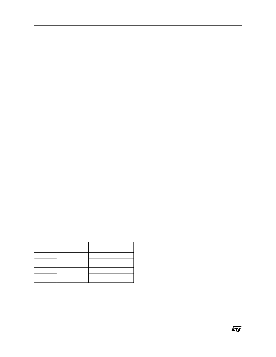
RCCR
Conditions
ST7L3
Addresses
RCCRH0
VDD = 5V
TA = 25°C
fRC = 1 MHz
DEE0h1) (CR[9:2] bits)
RCCRL0
DEE1h1) (CR[1:0] bits)
RCCRH1
VDD = 3.3V
TA = 25°C
fRC = 1 MHz
DEE2h1) (CR[9:2] bits)
RCCRL1
DEE3h1) (CR[1:0] bits)
1
相关PDF资料 |
PDF描述 |
|---|---|
| ST7PL38F2UCXXXRE | 8-BIT, MROM, 8 MHz, MICROCONTROLLER, QCC20 |
| ST7PL39F2MA/XXXE | 8-BIT, MROM, 8 MHz, MICROCONTROLLER, PDSO20 |
| ST7L38F2UC/XXXE | 8-BIT, MROM, 8 MHz, MICROCONTROLLER, QCC20 |
| ST7FL38F2UATRE | 8-BIT, FLASH, 8 MHz, MICROCONTROLLER, QCC20 |
| ST7PL35F2MAXXXRE | 8-BIT, MROM, 8 MHz, MICROCONTROLLER, PDSO20 |
相关代理商/技术参数 |
参数描述 |
|---|---|
| ST7PLITE02F0U6TR | 制造商:STMICROELECTRONICS 制造商全称:STMicroelectronics 功能描述:8-BIT MICROCONTROLLER WITH SINGLE VOLTAGE FLASH MEMORY, DATA EEPROM, ADC, TIMERS, SPI |
| ST7PLITE02Y0B6 | 制造商:STMICROELECTRONICS 制造商全称:STMicroelectronics 功能描述:8-BIT MICROCONTROLLER WITH SINGLE VOLTAGE FLASH MEMORY, DATA EEPROM, ADC, TIMERS, SPI |
| ST7PLITE02Y0B6TR | 制造商:STMICROELECTRONICS 制造商全称:STMicroelectronics 功能描述:8-bit microcontroller with single voltage Flash memory, data EEPROM, ADC, timers, SPI |
| ST7PLITE02Y0M6 | 制造商:STMICROELECTRONICS 制造商全称:STMicroelectronics 功能描述:8-bit microcontroller with single voltage Flash memory, data EEPROM, ADC, timers, SPI |
| ST7PLITE02Y0M6TR | 制造商:STMICROELECTRONICS 制造商全称:STMicroelectronics 功能描述:8-bit microcontroller with single voltage Flash memory, data EEPROM, ADC, timers, SPI |
发布紧急采购,3分钟左右您将得到回复。