- 您现在的位置:买卖IC网 > PDF目录3974 > UPD44647366AF5-E25-FQ1 (Renesas Electronics America)SRAM QDRII 72MBIT 165-PBGA PDF资料下载
参数资料
| 型号: | UPD44647366AF5-E25-FQ1 |
| 厂商: | Renesas Electronics America |
| 文件页数: | 28/42页 |
| 文件大小: | 0K |
| 描述: | SRAM QDRII 72MBIT 165-PBGA |
| 标准包装: | 1 |
| 格式 - 存储器: | RAM |
| 存储器类型: | SRAM - 同步,QDR II+ |
| 存储容量: | 72M(2M x 36) |
| 速度: | 400MHz |
| 接口: | 并联 |
| 电源电压: | 1.7 V ~ 1.9 V |
| 工作温度: | 0°C ~ 70°C |
| 封装/外壳: | 165-LBGA |
| 供应商设备封装: | 165-PBGA(13x15) |
| 包装: | 散装 |
第1页第2页第3页第4页第5页第6页第7页第8页第9页第10页第11页第12页第13页第14页第15页第16页第17页第18页第19页第20页第21页第22页第23页第24页第25页第26页第27页当前第28页第29页第30页第31页第32页第33页第34页第35页第36页第37页第38页第39页第40页第41页第42页
�� �
�
�μ� PD44647094A-A,� 44647184A-A,� 44647364A-A,� 44647096A-A,� 44647186A-A,� 44647366A-A�
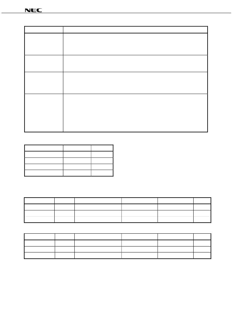
�Scan� Register� Definition� (1)�
�Register� name�
�Instruction� register�
�Bypass� register�
�ID� register�
�Boundary� register�
�Description�
�The� instruction� register� holds� the� instructions� that� are� executed� by� the� TAP� controller� when� it� is�
�moved� into� the� run-test/idle� or� the� various� data� register� state.� The� register� can� be� loaded� when� it� is�
�placed� between� the� TDI� and� TDO� pins.� The� instruction� register� is� automatically� preloaded� with� the�
�IDCODE� instruction� at� power-up� whenever� the� controller� is� placed� in� test-logic-reset� state.�
�The� bypass� register� is� a� single� bit� register� that� can� be� placed� between� TDI� and� TDO.� It� allows� serial�
�test� data� to� be� passed� through� the� RAMs� TAP� to� another� device� in� the� scan� chain� with� as� little� delay�
�as� possible.�
�The� ID� Register� is� a� 32� bit� register� that� is� loaded� with� a� device� and� vendor� specific� 32� bit� code� when�
�the� controller� is� put� in� capture-DR� state� with� the� IDCODE� command� loaded� in� the� instruction� register.�
�The� register� is� then� placed� between� the� TDI� and� TDO� pins� when� the� controller� is� moved� into� shift-DR�
�state.�
�The� boundary� register,� under� the� control� of� the� TAP� controller,� is� loaded� with� the� contents� of� the�
�RAMs� I/O� ring� when� the� controller� is� in� capture-DR� state� and� then� is� placed� between� the� TDI� and�
�TDO� pins� when� the� controller� is� moved� to� shift-DR� state.� Several� TAP� instructions� can� be� used� to�
�activate� the� boundary� register.�
�The� Scan� Exit� Order� tables� describe� which� device� bump� connects� to� each� boundary� register�
�location.� The� first� column� defines� the� bit’s� position� in� the� boundary� register.� The� second� column� is�
�the� name� of� the� input� or� I/O� at� the� bump� and� the� third� column� is� the� bump� number.�
�Scan� Register� Definition� (2)�
�Register� name�
�Instruction� register�
�Bypass� register�
�ID� register�
�Boundary� register�
�Bit� size�
�3�
�1�
�32�
�109�
�Unit�
�bit�
�bit�
�bit�
�bit�
�ID� Register� Definition�
�2.0� Clock� Cycles� Read� Latency�
�Part� number�
�μ� PD44647094A-A�
�μ� PD44647184A-A�
�μ� PD44647364A-A�
�Organization�
�8M� x� 9�
�4M� x� 18�
�2M� x� 36�
�ID� [31:28]� vendor� revision� no.�
�XXXX�
�XXXX�
�XXXX�
�ID� [27:12]� part� no.�
�0000� 0000� 1001� 0101�
�0000� 0000� 1001� 0110�
�0000� 0000� 1001� 0111�
�ID� [11:1]� vendor� ID� no.�
�00000010000�
�00000010000�
�00000010000�
�ID� [0]� fix� bit�
�1�
�1�
�1�
�2.5� Clock� Cycles� Read� Latency�
�Part� number�
�μ� PD44647096A-A�
�μ� PD44647186A-A�
�μ� PD44647366A-A�
�Organization�
�8M� x� 9�
�4M� x� 18�
�2M� x� 36�
�ID� [31:28]� vendor� revision� no.�
�XXXX�
�XXXX�
�XXXX�
�ID� [27:12]� part� no.�
�0000� 0000� 1010� 0001�
�0000� 0000� 1010� 0010�
�0000� 0000� 1010� 0011�
�ID� [11:1]� vendor� ID� no.�
�00000010000�
�00000010000�
�00000010000�
�ID� [0]� fix� bit�
�1�
�1�
�1�
�26�
�Data� Sheet� M19962EJ2V0DS�
�相关PDF资料 |
PDF描述 |
|---|---|
| MC7448HX1400NC | IC MPU RISC 32BIT 360-FCCBGA |
| UPD44647186AF5-E25-FQ1-A | SRAM QDRII 72MBIT 165-PBGA |
| UPD44647186AF5-E25-FQ1 | SRAM QDRII 72MBIT 165-PBGA |
| UPD44646363AF5-E25-FQ1-A | SRAM DDRII 72MBIT 165-PBGA |
| UPD44646363AF5-E25-FQ1 | SRAM DDRII 72MBIT 165-PBGA |
相关代理商/技术参数 |
参数描述 |
|---|---|
| UPD44647366AF5-E25-FQ1-A | 功能描述:SRAM QDRII 72MBIT 165-PBGA RoHS:是 类别:集成电路 (IC) >> 存储器 系列:- 标准包装:3,000 系列:- 格式 - 存储器:EEPROMs - 串行 存储器类型:EEPROM 存储容量:8K (1K x 8) 速度:400kHz 接口:I²C,2 线串口 电源电压:1.7 V ~ 5.5 V 工作温度:-40°C ~ 85°C 封装/外壳:8-SOIC(0.154",3.90mm 宽) 供应商设备封装:8-SOIC 包装:带卷 (TR) |
| UPD446C-2L | 制造商:NEC Electronics Corporation 功能描述:2K X 8 STANDARD SRAM, 200 ns, PDIP24 |
| UPD446G-20L | 制造商:NEC Electronics Corporation 功能描述:2K X 8 STANDARD SRAM, 200 ns, PDFP24 |
| UPD45128163G5 | 制造商:Renesas Electronics Corporation 功能描述:128 MBIT SDRAM |
| UPD45128163G5-A75-9JF | 制造商:Elpida Memory Inc 功能描述:8M X 16 SYNCHRONOUS DRAM, 5.4 ns, PDSO54 |
发布紧急采购,3分钟左右您将得到回复。