- 您现在的位置:买卖IC网 > PDF目录68559 > W972GG8JB-25I (WINBOND ELECTRONICS CORP) 256M X 8 DDR DRAM, 0.4 ns, PBGA60 PDF资料下载
参数资料
| 型号: | W972GG8JB-25I |
| 厂商: | WINBOND ELECTRONICS CORP |
| 元件分类: | DRAM |
| 英文描述: | 256M X 8 DDR DRAM, 0.4 ns, PBGA60 |
| 封装: | 11 X 11.50 MM, ROHS COMPLIANT, WBGA-60 |
| 文件页数: | 13/86页 |
| 文件大小: | 1466K |
| 代理商: | W972GG8JB-25I |
第1页第2页第3页第4页第5页第6页第7页第8页第9页第10页第11页第12页当前第13页第14页第15页第16页第17页第18页第19页第20页第21页第22页第23页第24页第25页第26页第27页第28页第29页第30页第31页第32页第33页第34页第35页第36页第37页第38页第39页第40页第41页第42页第43页第44页第45页第46页第47页第48页第49页第50页第51页第52页第53页第54页第55页第56页第57页第58页第59页第60页第61页第62页第63页第64页第65页第66页第67页第68页第69页第70页第71页第72页第73页第74页第75页第76页第77页第78页第79页第80页第81页第82页第83页第84页第85页第86页
W972GG8JB
Publication Release Date: Feb. 18, 2011
- 20 -
Revision A02
7.3
Command Function
7.3.1
Bank Activate Command
( CS ="L", RAS ="L", CAS ="H",
WE ="H", BA0, BA1, BA2=Bank, A0 to A14 be row address)
The Bank Activate command must be applied before any Read or Write operation can be executed.
Immediately after the bank active command, the DDR2 SDRAM can accept a read or write command
on the following clock cycle. If a Read/Write command is issued to a bank that has not satisfied the
tRCDmin specification, then additive latency must be programmed into the device to delay when the
Read/Write command is internally issued to the device. The additive latency value must be chosen to
assure tRCDmin is satisfied. Additive latencies of 0, 1, 2, 3, 4, 5 and 6 are supported. Once a bank has
been activated it must be precharged before another Bank Activate command can be applied to the
same bank. The bank active and precharge times are defined as tRAS and tRP, respectively. The
minimum time interval between successive Bank Activate commands to the same bank is determined
by the RAS cycle time of the device (tRC). The minimum time interval between Bank Activate
commands is tRRD.
In order to ensure that components with 8 internal memory banks do not exceed the instantaneous
current supplying capability, certain restrictions on operation of the 8 banks must be observed. There
are two rules. One for restricting the number of sequential ACT commands that can be issued and
another for allowing more time for RAS precharge for a Precharge All command. The rules are as
follows:
Sequential Bank Activation Restriction: No more than 4 banks may be activated in a rolling tFAW
window. Converting to clocks is done by dividing tFAW[nS] by tCK(avg)[ns], and rounding up to
next integer value. As an example of the rolling window, if RU{ (tFAW / tCK(avg) } is 10 clocks,
and an activate command is issued in clock N, no more than three further activate commands
may be issued at or between clock N+1 and N+9.
Precharge All Allowance: tRP for a Precharge All command is equal to tnRP + 1 x nCK, where
tnRP = RU{ tRP / tCK(avg) } and tRP is the value for a single bank precharge.
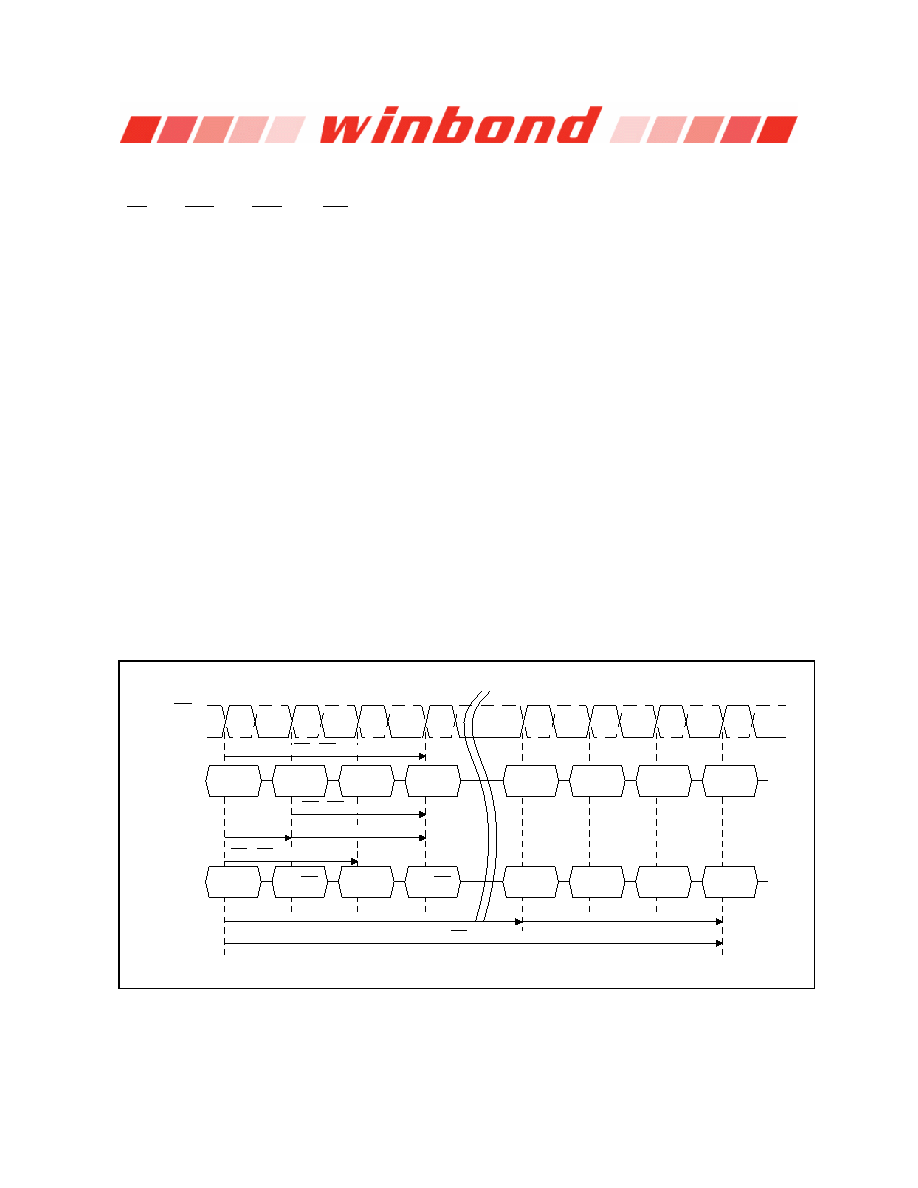
T0
T1
T2
T3
Tn
Tn+1
Tn+2
Tn+3
Bank A
Row Addr.
Bank A
Col. Addr.
Bank B
Row Addr.
Bank B
Col. Addr.
Bank A
Addr.
Bank B
Addr.
Bank A
Row Addr.
CAS - CAS delay time(tCCD)
tRCD = 1
Additive Latency delay(AL)
Read Begins
Bank A
Activate
Bank A
Post CAS
Read
Bank B
Activate
Bank B
Post CAS
Read
Bank A
Precharge
Bank B
Precharge
Bank A
Activate
Bank Active (
≥ tRAS)
RAS Cycle time (
≥ tRC)
Bank Precharge time (
≥ tRP)
Command
Address
RAS - RAS delay time(
≥ tRRD)
CLK
Internal RAS - RAS delay (
≥ tRCDmin)
Figure 12
– Bank activate command cycle: tRCD = 3, AL = 2, tRP = 3, tRRD = 2, tCCD = 2
相关PDF资料 |
PDF描述 |
|---|---|
| W972GG8JB-18 | 256M X 8 DDR DRAM, 0.35 ns, PBGA60 |
| W9751G6JB-18 | 32M X 16 DDR DRAM, 0.35 ns, PBGA84 |
| W981204AH-8H | 32M X 4 SYNCHRONOUS DRAM, 6 ns, PDSO54 |
| W981216BH75L | 8M X 16 SYNCHRONOUS DRAM, 5.4 ns, PDSO54 |
| W981216BH-75 | 8M X 16 SYNCHRONOUS DRAM, 5.4 ns, PDSO54 |
相关代理商/技术参数 |
参数描述 |
|---|---|
| W972GG8JB-3 | 制造商:Winbond Electronics Corp 功能描述:DRAM Chip DDR2 SDRAM 2G-Bit 256Mx8 1.8V 60-Pin WBGA 制造商:Winbond Electronics Corp 功能描述:IC DDR2 SDRAM 2GBIT 3NS |
| W9751G6IB-25 | 功能描述:IC DDR2-800 SDRAM 512MB 84-WBGA RoHS:是 类别:集成电路 (IC) >> 存储器 系列:- 标准包装:1,000 系列:- 格式 - 存储器:EEPROMs - 串行 存储器类型:EEPROM 存储容量:4K (512 x 8) 速度:400kHz 接口:I²C,2 线串口 电源电压:2.7 V ~ 5.5 V 工作温度:-40°C ~ 85°C 封装/外壳:8-SOIC(0.173",4.40mm 宽) 供应商设备封装:8-MFP 包装:带卷 (TR) |
| W9751G6JB | 制造商:WINBOND 制造商全称:Winbond 功能描述:8M ? 4 BANKS ? 16 BIT DDR2 SDRAM |
| W9751G6JB-25 | 制造商:Winbond Electronics Corp 功能描述:512GB DDRII |
| W9751G6JB-3 | 制造商:Winbond Electronics Corp 功能描述:512MB DDRII |
发布紧急采购,3分钟左右您将得到回复。