- 您现在的位置:买卖IC网 > PDF目录68559 > W972GG8JB-25I (WINBOND ELECTRONICS CORP) 256M X 8 DDR DRAM, 0.4 ns, PBGA60 PDF资料下载
参数资料
| 型号: | W972GG8JB-25I |
| 厂商: | WINBOND ELECTRONICS CORP |
| 元件分类: | DRAM |
| 英文描述: | 256M X 8 DDR DRAM, 0.4 ns, PBGA60 |
| 封装: | 11 X 11.50 MM, ROHS COMPLIANT, WBGA-60 |
| 文件页数: | 67/86页 |
| 文件大小: | 1466K |
| 代理商: | W972GG8JB-25I |
第1页第2页第3页第4页第5页第6页第7页第8页第9页第10页第11页第12页第13页第14页第15页第16页第17页第18页第19页第20页第21页第22页第23页第24页第25页第26页第27页第28页第29页第30页第31页第32页第33页第34页第35页第36页第37页第38页第39页第40页第41页第42页第43页第44页第45页第46页第47页第48页第49页第50页第51页第52页第53页第54页第55页第56页第57页第58页第59页第60页第61页第62页第63页第64页第65页第66页当前第67页第68页第69页第70页第71页第72页第73页第74页第75页第76页第77页第78页第79页第80页第81页第82页第83页第84页第85页第86页
W972GG8JB
Publication Release Date: Feb. 18, 2011
- 7 -
Revision A02
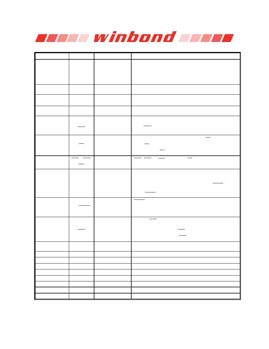
5.
BALL DESCRIPTION
BALL NUMBER
SYMBOL
FUNCTION
DESCRIPTION
H8,H3,H7,J2,J8,J3,
J7,K2,K8,K3,H2,K7,
L2,L8,L3
A0
A14
Address
Provide the row address for active commands, and the column
address and Auto-precharge bit for Read/Write commands to select
one location out of the memory array in the respective bank.
Row address: A0
A14.
Column address: A0
A9. (A10 is used for Auto-precharge)
G2,G3,G1
BA0
BA2
Bank Select
BA0
BA2 define to which bank an ACTIVE, READ, WRITE or
PRECHARGE command is being applied.
C8,C2,D7,D3,D1,D9,
B1,B9
DQ0
DQ7
Data Input
/ Output
Bi-directional data bus.
F9
ODT
On Die Termination
Control
ODT (registered HIGH) enables termination resistance internal to
the DDR2 SDRAM.
B7,A8
DQS,
DQS
Data Strobe /
Differential Read Data
Strobe
Output with read data, input with write data for source synchronous
operation. Edge-aligned with read data, center-aligned with write
data. DQS is only used when differential data strobe mode is
enabled via the control bit at EMR (1) [A10] = 0.
G8
CS
Chip Select
All
commands
are
masked
when
CS
is
registered
HIGH
. CS provides for external Rank selection on systems with
multiple Ranks.
CS is considered part of the command code.
F7,G7,F3
RAS , CAS ,
WE
Command Inputs
RAS , CAS and WE (along with CS ) define the command being
entered.
B3
DM/RDQS
Input Data Mask/
Read Data Strobe
DM is an input mask signal for write data. Input data is masked
when DM is sampled HIGH coincident with that input data during a
Write access. DM is sampled on both edges of DQS. The DM
loading matches the DQ and DQS loading. RDQS/ RDQS are used
as strobe signals during reads is enabled by EMR (1) [A11] = 1. If
RDQS/ RDQS is enabled, the DM function is disabled.
A2
NU/ RDQS
Not Use/Differential
Read Data Strobe
RDQS is only used when RDQS is enabled and differential data
strobe mode is enabled. If differential data strobe mode is disabled
via the control bit at EMR (1) [A10] = 1, then ball A2 and A8 are not
used.
E8,F8
CLK,
CLK
Differential Clock
Inputs
CLK and
CLK are differential clock inputs. All address and control
input signals are sampled on the crossing of the positive edge of
CLK and negative edge of
CLK . Output (read) data is referenced
to the crossings of CLK and
CLK (both directions of crossing).
F2
CKE
Clock Enable
CKE (registered HIGH) activates and CKE (registered LOW)
deactivates clocking circuitry on the DDR2 SDRAM.
E2
VREF
Reference Voltage
VREF is reference voltage for inputs.
A1,E9,H9,L1
VDD
Power Supply
Power Supply: 1.8V
0.1V.
A3,E3,J1,K9
VSS
Ground
Ground.
A9,C1,C3,C7,C9
VDDQ
DQ Power Supply
DQ Power Supply: 1.8V
0.1V.
A7,B2,B8,D2,D8
VSSQ
DQ Ground
DQ Ground. Isolated on the device for improved noise immunity.
L3,L7
NC
No Connection
No connection.
E1
VDDL
DLL Power Supply
DLL Power Supply: 1.8V
0.1V.
E7
VSSDL
DLL Ground
DLL Ground.
相关PDF资料 |
PDF描述 |
|---|---|
| W972GG8JB-18 | 256M X 8 DDR DRAM, 0.35 ns, PBGA60 |
| W9751G6JB-18 | 32M X 16 DDR DRAM, 0.35 ns, PBGA84 |
| W981204AH-8H | 32M X 4 SYNCHRONOUS DRAM, 6 ns, PDSO54 |
| W981216BH75L | 8M X 16 SYNCHRONOUS DRAM, 5.4 ns, PDSO54 |
| W981216BH-75 | 8M X 16 SYNCHRONOUS DRAM, 5.4 ns, PDSO54 |
相关代理商/技术参数 |
参数描述 |
|---|---|
| W972GG8JB-3 | 制造商:Winbond Electronics Corp 功能描述:DRAM Chip DDR2 SDRAM 2G-Bit 256Mx8 1.8V 60-Pin WBGA 制造商:Winbond Electronics Corp 功能描述:IC DDR2 SDRAM 2GBIT 3NS |
| W9751G6IB-25 | 功能描述:IC DDR2-800 SDRAM 512MB 84-WBGA RoHS:是 类别:集成电路 (IC) >> 存储器 系列:- 标准包装:1,000 系列:- 格式 - 存储器:EEPROMs - 串行 存储器类型:EEPROM 存储容量:4K (512 x 8) 速度:400kHz 接口:I²C,2 线串口 电源电压:2.7 V ~ 5.5 V 工作温度:-40°C ~ 85°C 封装/外壳:8-SOIC(0.173",4.40mm 宽) 供应商设备封装:8-MFP 包装:带卷 (TR) |
| W9751G6JB | 制造商:WINBOND 制造商全称:Winbond 功能描述:8M ? 4 BANKS ? 16 BIT DDR2 SDRAM |
| W9751G6JB-25 | 制造商:Winbond Electronics Corp 功能描述:512GB DDRII |
| W9751G6JB-3 | 制造商:Winbond Electronics Corp 功能描述:512MB DDRII |
发布紧急采购,3分钟左右您将得到回复。