参数资料
| 型号: | XRD98L63AIV-F |
| 厂商: | Exar Corporation |
| 文件页数: | 24/41页 |
| 文件大小: | 0K |
| 描述: | IC CCD DIGITIZER 12BIT 48TQFP |
| 标准包装: | 250 |
| 位数: | 12 |
| 通道数: | 1 |
| 电压 - 电源,模拟: | 2.7 V ~ 3.6 V |
| 电压 - 电源,数字: | 2.7 V ~ 3.6 V |
| 封装/外壳: | 48-TQFP |
| 供应商设备封装: | 48-TQFP(7x7) |
| 包装: | 托盘 |
第1页第2页第3页第4页第5页第6页第7页第8页第9页第10页第11页第12页第13页第14页第15页第16页第17页第18页第19页第20页第21页第22页第23页当前第24页第25页第26页第27页第28页第29页第30页第31页第32页第33页第34页第35页第36页第37页第38页第39页第40页第41页
XRD98L63
30
Rev.1.01
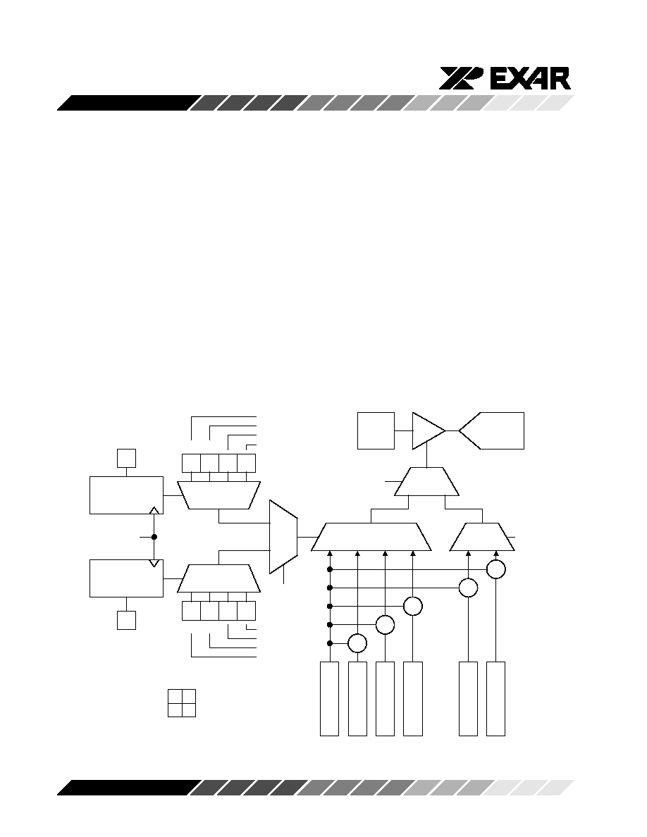
MULTIPLE GAIN MODE
The Benefits of Multiple Gain Mode
The Multiple Gain mode switches the gain of the
Programmable Gain Amplifier (PGA) at the pixel rate.
The Multiple Gain logic will switch the PGA gain
according to two user defined patterns. Each pattern
can be from one to four pixels long.
This allows a color digital camera system to set
different PGA (analog) gains for the different color
pixels. Most CCDs with RGB Color Filter Arrays (CFA)
have weaker signal response for the Blue pixels than for
Red or Green pixels. Using the Multiple Gain mode, the
Blue pixels can be amplified with higher gain than the
Red or Green pixels before being digitized by the ADC.
This allows all colors to take advantage of the full ADC
resolution.
Enable the Multiple Gain mode by writing a "1" to the
"MultGain" bit in the Control register.
Overview of Multiple Gain Mode
The Multiple Gain mode is designed assuming the color
filter array is made up of lines (rows) which alternate
between two different pixel patterns. We will refer to the
two patterns as the Even pattern and the Odd pattern.
In a typical camera design using an RGB CFA, the even
lines will have Red & Green alternating pixels, while the
Odd lines will have Green & Blue alternating pixels. The
XRD98L63 allows the patterns to be defined with a
single Green gain used on both Even and Odd lines, or
with two different Green gains for Even and Odd lines.
There are three main steps to setting up and using the
Multiple Gain mode:
1)
Select the appropriate Interlaced or Progressive
scan clocking mode.
2)
Program the Even and Odd Line Pattern registers
to match the color filter array used on the CCD.
3)
Program the Gain Registers.
L
in
e
P
a
tt
e
rn
S
e
le
c
t
PRE[1:0]
Even Line Pattern
Line
Pattern
Se lect
CAL
SBLK
P
G
A
0
M
a
s
te
r
R
Gb
Gr
B
P
G
A
0
1
D
if
fe
re
n
c
e
P
G
A
1
0
D
if
fe
re
n
c
e
P
G
A
1
D
if
fe
re
n
c
e
O
B
E
v
e
n
G
a
in
O
B
O
d
G
a
in
Σ
+
+
+
+
+
00
PGA mux
01
10
11
CDS
ADC
PGA
0
1
01
PRO [1:0]
Even Pixel Repeat
Counter
0 to PRE[1:0]
Odd Pixel Repeat
Counter
0 to PRO[1:0]
R
Gr
10
11
00
01
10
11
Gb
B
00
01
00
01
10
11
01
ELP4[1:0]
ELP3[1:0]
ELP2[1:0]
ELP1[1:0]
Odd Line Pattern
OLP4[1:0]
OLP3[1:0]
OLP2[1:0]
OLP1[1:0]
even pattern
odd pattern
Examp le pattern
R
Gr
Gb B
Figure 24. Block Diagram of the Multiple Gain Logic
相关PDF资料 |
PDF描述 |
|---|---|
| XRT71D00IQ-F | IC JITTER ATTENUATOR SGL 32TQFP |
| XRT71D03IV-F | IC JITTER ATTENUATOR 3CH 64TQFP |
| XRT71D04IV | IC JITTER ATTENUATOR 4CH 80TQFP |
| XRT8000IP-F | IC WAN CLOCK E1/E1 DUAL 18PDIP |
| XRT8001IP-F | IC WAN CLOCK E1/E1 DUAL 18PDIP |
相关代理商/技术参数 |
参数描述 |
|---|---|
| XRD98L63AIVTR-F | 制造商:Exar Corporation 功能描述:AFE General Purpose 1ADC 12-Bit 3V 48-Pin TQFP T/R 制造商:Exar Corporation 功能描述:XRD98L63AIVTR-F |
| XRD98L63EVAL | 功能描述:数据转换 IC 开发工具 Eval Board for XRD98L63AIV RoHS:否 制造商:Texas Instruments 产品:Demonstration Kits 类型:ADC 工具用于评估:ADS130E08 接口类型:SPI 工作电源电压:- 6 V to + 6 V |
| XRD98L63ZEVAL | 功能描述:数据转换 IC 开发工具 Eval Board (Solder) XRD98L63AIV RoHS:否 制造商:Texas Instruments 产品:Demonstration Kits 类型:ADC 工具用于评估:ADS130E08 接口类型:SPI 工作电源电压:- 6 V to + 6 V |
| XRDAN27 | 制造商:EXAR 制造商全称:EXAR 功能描述:Compensating for Zero Order Hold Effects |
| XRDAN28 | 制造商:EXAR 制造商全称:EXAR 功能描述:Frequency Response Effects of Overampling and Averaging on A/D Output Data |
发布紧急采购,3分钟左右您将得到回复。