参数资料
| 型号: | XRD98L63AIV-F |
| 厂商: | Exar Corporation |
| 文件页数: | 3/41页 |
| 文件大小: | 0K |
| 描述: | IC CCD DIGITIZER 12BIT 48TQFP |
| 标准包装: | 250 |
| 位数: | 12 |
| 通道数: | 1 |
| 电压 - 电源,模拟: | 2.7 V ~ 3.6 V |
| 电压 - 电源,数字: | 2.7 V ~ 3.6 V |
| 封装/外壳: | 48-TQFP |
| 供应商设备封装: | 48-TQFP(7x7) |
| 包装: | 托盘 |
第1页第2页当前第3页第4页第5页第6页第7页第8页第9页第10页第11页第12页第13页第14页第15页第16页第17页第18页第19页第20页第21页第22页第23页第24页第25页第26页第27页第28页第29页第30页第31页第32页第33页第34页第35页第36页第37页第38页第39页第40页第41页
11
Rev.1.01
XRD98L63
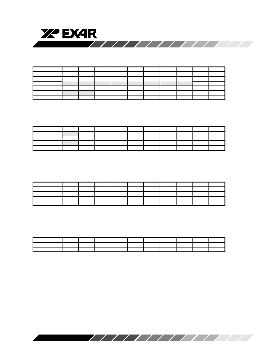
Wait A, Wait B and OB Lines Registers
D9
D8
D7
D6
D5
D4
D3
D2
D1
D0
WaitA
WL[11]
WL[10]
WL[9]
WL[8]
WL[7]
WL[6]
WL[5]
WL[4]
WL[3]
WL[2]
default
0
WaitB
WL[1]
WL[0]
default
0
1
OB Lines
OBL[7]
OBL[6]
OBL[5]
OBL[4]
OBL[3]
OBL[2]
OBL[1]
OBL[0]
default
0
1
0
1
0
WL[11:0] and OBL[7:0] are used by the Black Level Calibration logic in the Frame mode to determine which
lines to use for Calibration. (Frame mode is not currently supported)
See the “Black Level Offset Calibration” section (pg. 19) for more information.
CDAC Even and CDAC Odd Registers
D9
D8
D7
D6
D5
D4
D3
D2
D1
D0
CDAC Even
CDE[8]
CDE[7]
CDE[6]
CDE[5]
CDE[4]
CDE[3]
CDE[2]
CDE[1]
CDE[0]
default
0
CDAC Odd
CDO[8]
CDO[7]
CDO[6]
CDO[5]
CDO[4]
CDO[3]
CDO[2]
CDO[1]
CDO[0]
default
0
CDE[8:0] and CDO[8:0] are used to program the internal Coarse Offset DAC in the Manual Calibration
mode. In the normal, single gain mode the value in CDE[8:0] is used. In the Multiple Gain mode, CDE[8:0] is
used for Even lines and CDO[8:0] is used for Odd lines.
See the “Black Level Offset Calibration” section (pg. 19) for more information.
FDAC Even and FDAC Odd Registers
D9
D8
D7
D6
D5
D4
D3
D2
D1
D0
FDAC Even
FDE[9]
FDE[8]
FDE[7]
FDE[6]
FDE[5]
FDE[4]
FDE[3]
FDE[2]
FDE[1]
FDE[0]
default
0
FDAC Odd
FDO[9]
FDO[8]
FDO[7]
FDO[6]
FDO[5]
FDO[4]
FDO[3]
FDO[2]
FDO[1]
FDO[0]
default
0
FDE[9:0] and FDO[9:0] are used to program the internal Fine Offset DAC in the Manual Calibration mode. In
the normal, single gain mode the value in FDE[9:0] is used. In the Multiple Gain mode, FDE[9:0] is used for
Even lines and FDO[9:0] is used for Odd lines.
See the “Black Level Offset Calibration” section (pg. 19) for more information.
Control Register
D9
D8
D7
D6
D5
D4
D3
D2
D1
D0
Control
ADCpd
AFEpd
CHIPpd
OE
MultGain
MGsel[1]
MGsel[0]
MGstart
MinClip
OneV
default
0
1
0
1
0
The Control register is used to program various options.
ADCpd, power down the ADC block. 0=normal operation. 1=ADC power down.
AFEpd, power down the AFE block. 0=normal operation. 1=AFE power down.
OE, output enable control. 0=DB[11:0] in high Z mode. 1=DB[11:0] in active drive mode.
MultGain, enable the Multiple Gain mode. 0=single gain mode. 1= Multiple Gain mode.
MGsel[1:0], Multiple Gain timing mode select.
MGstart, Even or Odd starting condition for MGsel[1:0]=11. 0=start with Even line, 1=start with Odd line.
MinClip, minimum clip option. 0=minimum clip disabled, 1=minimum clip enabled.
OneV, 1 volt input range option. 0=0.8V maximum input range. 1=1.0V maximum input range.
See the “Chip Power Down” section (pg. 34) for information about ADCpd, AFEpd, CHIPpd and OE.
See the “Multiple Gain Mode” section (pg. 30) for information about MultGain, MGsel[1:0] and MGstart.
See the “Other Chip Controls and Features” section (pg. 34) for information about MinClip.
See the “One Volt Input Option” section (pg. 16) for information about OneV.
相关PDF资料 |
PDF描述 |
|---|---|
| XRT71D00IQ-F | IC JITTER ATTENUATOR SGL 32TQFP |
| XRT71D03IV-F | IC JITTER ATTENUATOR 3CH 64TQFP |
| XRT71D04IV | IC JITTER ATTENUATOR 4CH 80TQFP |
| XRT8000IP-F | IC WAN CLOCK E1/E1 DUAL 18PDIP |
| XRT8001IP-F | IC WAN CLOCK E1/E1 DUAL 18PDIP |
相关代理商/技术参数 |
参数描述 |
|---|---|
| XRD98L63AIVTR-F | 制造商:Exar Corporation 功能描述:AFE General Purpose 1ADC 12-Bit 3V 48-Pin TQFP T/R 制造商:Exar Corporation 功能描述:XRD98L63AIVTR-F |
| XRD98L63EVAL | 功能描述:数据转换 IC 开发工具 Eval Board for XRD98L63AIV RoHS:否 制造商:Texas Instruments 产品:Demonstration Kits 类型:ADC 工具用于评估:ADS130E08 接口类型:SPI 工作电源电压:- 6 V to + 6 V |
| XRD98L63ZEVAL | 功能描述:数据转换 IC 开发工具 Eval Board (Solder) XRD98L63AIV RoHS:否 制造商:Texas Instruments 产品:Demonstration Kits 类型:ADC 工具用于评估:ADS130E08 接口类型:SPI 工作电源电压:- 6 V to + 6 V |
| XRDAN27 | 制造商:EXAR 制造商全称:EXAR 功能描述:Compensating for Zero Order Hold Effects |
| XRDAN28 | 制造商:EXAR 制造商全称:EXAR 功能描述:Frequency Response Effects of Overampling and Averaging on A/D Output Data |
发布紧急采购,3分钟左右您将得到回复。