- 您现在的位置:买卖IC网 > PDF目录17316 > ZL2106EVAL1Z (Intersil)BOARD EVAL STEP-DOWN ZL2106 PDF资料下载
参数资料
| 型号: | ZL2106EVAL1Z |
| 厂商: | Intersil |
| 文件页数: | 24/29页 |
| 文件大小: | 0K |
| 描述: | BOARD EVAL STEP-DOWN ZL2106 |
| 标准包装: | 1 |
| 系列: | Zilker Labs™ |
| 主要目的: | DC/DC,步降 |
| 输出及类型: | 1,非隔离 |
| 输出电压: | 3.3V |
| 电流 - 输出: | 6A |
| 输入电压: | 12V |
| 稳压器拓扑结构: | 降压 |
| 频率 - 开关: | 400kHz |
| 板类型: | 完全填充 |
| 已供物品: | 板 |
| 已用 IC / 零件: | ZL2106 |
第1页第2页第3页第4页第5页第6页第7页第8页第9页第10页第11页第12页第13页第14页第15页第16页第17页第18页第19页第20页第21页第22页第23页当前第24页第25页第26页第27页第28页第29页
�� �
�
�ZL2106�
�Phase� Spreading�
�When� multiple� point� of� load� converters� share� a� common� DC�
�input� supply,� it� is� desirable� to� adjust� the� clock� phase� offset� of�
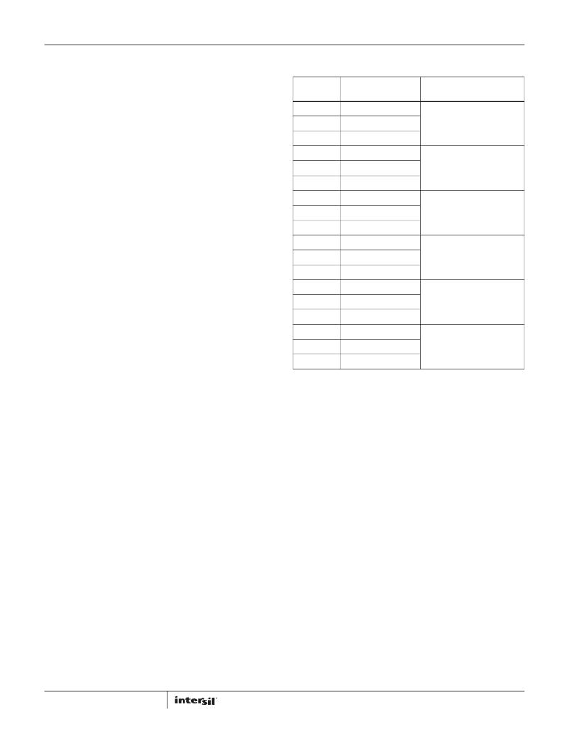
�TABLE� 16.� CFG� PIN� CONFIGURATIONS� FOR� SEQUENCING� AND�
�TRACKING�
�SYNC� PIN�
�each� device� such� that� not� all� devices� start� to� switch�
�simultaneously.� Setting� each� converter� to� start� its� switching� cycle�
�at� a� different� point� in� time� can� dramatically� reduce� input�
�capacitance� requirements� and� efficiency� losses.� Since� the� peak�
�current� drawn� from� the� input� supply� is� effectively� spread� out� over�
�a� period� of� time,� the� peak� current� drawn� at� any� given� moment� is�
�reduced� and� the� power� losses� proportional� to� the� I� RMS2� are�
�reduced� dramatically.�
�In� order� to� enable� phase� spreading,� all� converters� must� be�
�synchronized� to� the� same� switching� clock.� The� CFG� pin� is� used� to�
�set� the� configuration� of� the� SYNC� pin� for� each� device� as�
��Selecting� the� phase� offset� for� the� device� is� accomplished� by�
�selecting� a� device� address� according� to� the� following� equation:�
�Phase� offset� =� device� address� x� 45°�
�For� example:�
�?� A� device� address� of� 0x00� or� 0x20� would� configure� no� phase�
�offset�
�?� A� device� address� of� 0x01� or� 0x21� would� configure� 45°� of�
�phase� offset�
�?� A� device� address� of� 0x02� or� 0x22� would� configure� 90°� of�
�phase� offset�
�R� CFG�
�Low�
�Open�
�High�
�10k� Ω�
�11k� Ω�
�12.1k� Ω�
�14.7k� Ω�
�16.2k� Ω�
�17.8k� Ω�
�21.5k� Ω�
�23.7k� Ω�
�26.1k� Ω�
�31.6k� Ω�
�34.8k� Ω�
�38.3k� Ω�
�46.4k� Ω�
�51.1k� Ω�
�CONFIGURATION�
�Input�
�Auto� detect�
�Output�
�Input�
�Auto� detect�
�Output�
�Input�
�Auto� detect�
�Output�
�Input�
�Auto� detect�
�Output�
�Input�
�Auto� detect�
�Output�
�Input�
�Auto� detect�
�SEQUENCING� CONFIGURATION�
�Sequencing� and� Tracking� are�
�disabled.�
�Sequencing� and� Tracking� are�
�disabled.�
�Device� is� FIRST� in� nested�
�sequence.� Tracking� disabled.�
�Device� is� LAST� in� nested�
�sequence.� Tracking� disabled.�
�Device� is� MIDDLE� in� nested�
�sequence.� Tracking� disabled.�
�Sequence� disabled.� Tracking�
�enabled� as� defined� in� Table� 13.�
�The� phase� offset� of� each� device� may� also� be� set� to� any� value�
�between� 0°� and� 360°� in� 22.5°� increments� via� the� I� 2� C/SMBus�
�interface.� Refer� to� Application� Note� AN2033� for� further� details.�
�Output� Sequencing�
�A� group� of� Zilker� Labs� devices� may� be� configured� to� power� up� in�
�a� predetermined� sequence.� This� feature� is� especially� useful� when�
�powering� advanced� processors,� FPGAs,� and� ASICs� that� require�
�one� supply� to� reach� its� operating� voltage� prior� to� another� supply�
�reaching� its� operating� voltage� in� order� to� avoid� latch-up� from�
�occurring.� Multi-device� sequencing� can� be� achieved� by�
�configuring� each� device� through� the� I� 2� C/SMBus� interface� or� by�
�using� Zilker� Labs� patented� autonomous� sequencing� mode.�
�Autonomous� sequencing� mode� configures� sequencing� by� using�
�events� transmitted� between� devices� over� the� DDC� bus.�
�The� sequencing� order� is� determined� using� each� device’s� SMBus�
�address.� Using� autonomous� sequencing� mode� (configured� using�
�the� CFG� pin),� the� devices� must� be� assigned� sequential� SMBus�
�addresses� with� no� missing� addresses� in� the� chain.� This� mode� will�
�also� constrain� each� device� to� have� a� phase� offset� according� to� its�
���24�
�56.2k� Ω� Output�
�The� sequencing� group� will� turn� on� in� order� starting� with� the�
�device� with� the� lowest� SMBus� address� and� will� continue� through�
�to� turn� on� each� device� in� the� address� chain� until� all� devices�
�connected� have� been� turned� on.� When� turning� off,� the� device�
�with� the� highest� SMBus� address� will� turn� off� first� followed� in�
�reverse� order� by� the� other� devices� in� the� group.�
�Sequencing� is� configured� by� connecting� a� resistor� from� the� CFG�
�pin� to� ground� as� described� in� Table� 16.� The� CFG� pin� is� also� used�
�to� set� the� configuration� of� the� SYNC� pin� as� well� as� to� determine�
�the� sequencing� method� and� order.� Please� refer� to� section�
��the� operating� parameters� of� the� SYNC� pin.�
�Multiple� device� sequencing� may� also� be� achieved� by� issuing�
�PMBus� commands� to� assign� the� preceding� device� in� the�
�sequencing� chain� as� well� as� the� device� that� will� follow� in� the�
�sequencing� chain.� This� method� places� fewer� restrictions� on� the�
�SMBus� address� (no� need� of� sequential� address)� and� also� allows�
�the� user� to� assign� any� phase� offset� to� any� device� irrespective� of�
�its� SMBus� device� address.�
�The� Enable� pins� of� all� devices� in� a� sequencing� group� must� be� tied�
�together� and� driven� high� to� initiate� a� sequenced� turn-on� of� the�
�group.� Enable� must� be� driven� low� to� initiate� a� sequenced� turnoff�
�of� the� group.� Please� refer� to� Application� Note� AN2033� for� details�
�on� sequencing� via� the� I� 2� C/SMBus� interface.�
�FN6852.6�
�February� 20,� 2013�
�相关PDF资料 |
PDF描述 |
|---|---|
| R1D-3.33.3/P-R | CONV DC/DC 1W 3.3VIN +/-3.3VOUT |
| A9BBA-1802F | FLEX CABLE - AFF18A/AF18/AFF18A |
| 195D685X9025Y2T | CAP TANT 6.8UF 25V 10% 2910 |
| R1D-3.33.3/H-R | CONV DC/DC 1W 3.3VIN +/-3.3VOUT |
| 195D685X0025Y2T | CAP TANT 6.8UF 25V 20% 2910 |
相关代理商/技术参数 |
参数描述 |
|---|---|
| ZL212 | 制造商:SMC Corporation of America 功能描述:Multistage Ejector,Rc 1/8 Supply,Rc 3/4 |
| ZL212-DPL | 制造商:SMC Corporation of America 功能描述:VACUUM EJECTOR, W/O VALVE |
| ZL212-G | 制造商:SMC Corporation of America 功能描述:Vacuum Ejector; 1.2 mm x 2; 0.5 m; 200 per minute (AVR); 126 per minute (ANR) |
| ZL22B | 制造商:YEASHIN 制造商全称:YEASHIN 功能描述:500 mW DO-35 Hermetically Sealed Glass Zener Voltage Regulators |
| ZL24605 | 制造商:Microsemi Corporation 功能描述:5 OUTPUT ANY-RATE LINE CARD TIMING IC - Bulk |
发布紧急采购,3分钟左右您将得到回复。