- 您现在的位置:买卖IC网 > PDF目录17316 > ZL2106EVAL1Z (Intersil)BOARD EVAL STEP-DOWN ZL2106 PDF资料下载
参数资料
| 型号: | ZL2106EVAL1Z |
| 厂商: | Intersil |
| 文件页数: | 6/29页 |
| 文件大小: | 0K |
| 描述: | BOARD EVAL STEP-DOWN ZL2106 |
| 标准包装: | 1 |
| 系列: | Zilker Labs™ |
| 主要目的: | DC/DC,步降 |
| 输出及类型: | 1,非隔离 |
| 输出电压: | 3.3V |
| 电流 - 输出: | 6A |
| 输入电压: | 12V |
| 稳压器拓扑结构: | 降压 |
| 频率 - 开关: | 400kHz |
| 板类型: | 完全填充 |
| 已供物品: | 板 |
| 已用 IC / 零件: | ZL2106 |
第1页第2页第3页第4页第5页当前第6页第7页第8页第9页第10页第11页第12页第13页第14页第15页第16页第17页第18页第19页第20页第21页第22页第23页第24页第25页第26页第27页第28页第29页
�� �
�
�ZL2106�
�Absolute� Maximum� Ratings�
�DC� Supply� Voltage� for� VDDP,� VDDS� Pins� .� .� .� .� .� .� .� .� .� .� .� .� .� .� .� .� .� .� -0.3V� to� 17V�
�High-Side� Supply� Voltage� for� BST� Pin.� .� .� .� .� .� .� .� .� .� .� .� .� .� .� .� .� .� .� .� .� -0.3V� to� 25V�
�High-Side� Boost� Voltage� for� BST� -� SW� Pins� .� .� .� .� .� .� .� .� .� .� .� .� .� .� .� .� .� -0.3V� to� 8V�
�Internal� MOSFET� Reference� for� VR� Pin� .� .� .� .� .� .� .� .� .� .� .� .� .� .� .� .� .� .� -0.3V� to� 8.5V�
�Internal� Analog� Reference� for� VRA� Pin� .� .� .� .� .� .� .� .� .� .� .� .� .� .� .� .� .� .� -0.3V� to� 6.5V�
�Internal� 2.5� V� Reference� for� V2P5� Pin.� .� .� .� .� .� .� .� .� .� .� .� .� .� .� .� .� .� .� .� .� -0.3V� to� 3V�
�Logic� I/O� Voltage� for� EN,� CFG,� DDC,� FC,� MGN,� PG,� SDA,� SCL,�
�SA,� SALRT,� SS,� SYNC,� VTRK,� VSET,� VSEN� Pins� .� .� .� .� .� .� .� .� .� .� -0.3V� to� 6.5V�
�Ground� Differential� for� DGND� -� SGND,�
�PGND� -� SGND� Pins� .� .� .� .� .� .� .� .� .� .� .� .� .� .� .� .� .� .� .� .� .� .� .� .� .� .� .� .� .� .� .� .� .� .� .� .� .� ±0.3V�
�MOSFET� Drive� Reference� Current� for� VR� Pin�
�Internal� Bias� Usage� .� .� .� .� .� .� .� .� .� .� .� .� .� .� .� .� .� .� .� .� .� .� .� .� .� .� .� .� .� .� .� .� .� .� .� .� .� .� 20mA�
�Switch� Node� Current� for� SW� Pin�
�Peak� (Sink� Or� Source)� .� .� .� .� .� .� .� .� .� .� .� .� .� .� .� .� .� .� .� .� .� .� .� .� .� .� .� .� .� .� .� .� .� .� .� .� .� .� 10A�
�ESD� Rating�
�Human� Body� Model� .� .� .� .� .� .� .� .� .� .� .� .� .� .� .� .� .� .� .� .� .� .� .� .� .� .� .� .� .� .� .� .� .� .� .� .� .� .� .� .� 2kV�
�Machine� Model� .� .� .� .� .� .� .� .� .� .� .� .� .� .� .� .� .� .� .� .� .� .� .� .� .� .� .� .� .� .� .� .� .� .� .� .� .� .� .� .� .� .� 500V�
�Latch-Up.� .� .� .� .� .� .� .� .� .� .� .� .� .� .� .� .� .� .� .� .� .� .� .� .� .� .� .� .� .� per� JESD78� (JEDEC� Standard)�
�Thermal� Information�
�Thermal� Resistance� (Typical)� θ� JA� (°C/W)� θ� JC� (°C/W)�
�36� Ld� QFN� (Notes� 4,� 5)� .� .� .� .� .� .� .� .� .� .� .� .� .� .� .� .� 28� 1.7�
�Junction� Temperature� Range� .� .� .� .� .� .� .� .� .� .� .� .� .� .� .� .� .� .� .� .� .� .� .-55°C� to� +150°C�
�Storage� Temperature� Range.� .� .� .� .� .� .� .� .� .� .� .� .� .� .� .� .� .� .� .� .� .� .� .-55°C� to� +150°C�
�Dissipation� Limits� (Note� 6)�
�T� A� =� +25°C� .� .� .� .� .� .� .� .� .� .� .� .� .� .� .� .� .� .� .� .� .� .� .� .� .� .� .� .� .� .� .� .� .� .� .� .� .� .� .� .� .� .� .� .� .� .� 3.5W�
�T� A� =� +55°C� .� .� .� .� .� .� .� .� .� .� .� .� .� .� .� .� .� .� .� .� .� .� .� .� .� .� .� .� .� .� .� .� .� .� .� .� .� .� .� .� .� .� .� .� .� .� 2.5W�
�T� A� =� +85°C� .� .� .� .� .� .� .� .� .� .� .� .� .� .� .� .� .� .� .� .� .� .� .� .� .� .� .� .� .� .� .� .� .� .� .� .� .� .� .� .� .� .� .� .� .� .� 1.4W�
�Pb-Free� Reflow� Profile� .� .� .� .� .� .� .� .� .� .� .� .� .� .� .� .� .� .� .� .� .� .� .� .� .� .� .� .� .� .� .� see� link� below�
��Recommended� Operating� Conditions�
�Input� Supply� Voltage� Range,� VDDP,� VDDS� (See� Figure� 14)�
�VDDS� tied� to� VR,� VRA� .� .� .� .� .� .� .� .� .� .� .� .� .� .� .� .� .� .� .� .� .� .� .� .� .� .� .� .� .� .� .� .� 4.5V� to� 5.5V�
�VDDS� tied� to� VR,� VRA� Floating� .� .� .� .� .� .� .� .� .� .� .� .� .� .� .� .� .� .� .� .� .� .� .� .� 5.5V� to� 7.5V�
�VR,� VRA� Floating.� .� .� .� .� .� .� .� .� .� .� .� .� .� .� .� .� .� .� .� .� .� .� .� .� .� .� .� .� .� .� .� .� .� .� .� .7.5V� to� 14V�
�Output� Voltage� Range,� V� OUT� (Note� 7)� .� .� .� .� .� .� .� .� .� .� .� .� .� .� .� .� .� .� .� .� 0.54V� to� 5.5V�
�Operating� Junction� Temperature� Range,� T� J� .� .� .� .� .� .� .� .� .� .� .� .� .-40°C� to� +125°C�
�CAUTION:� Do� not� operate� at� or� near� the� maximum� ratings� listed� for� extended� periods� of� time.� Exposure� to� such� conditions� may� adversely� impact� product�
�reliability� and� result� in� failures� not� covered� by� warranty.�
�NOTES:�
�4.� θ� JA� is� measured� in� free� air� with� the� component� mounted� on� a� high� effective� thermal� conductivity� test� board� with� “direct� attach”� features.� See� Tech�
��5.� For� θ� JC� ,� the� “case� temp”� location� is� the� center� of� the� exposed� metal� pad� on� the� package� underside.�
�6.� Thermal� impedance� depends� on� layout.�
�7.� Includes� margin� limits.�
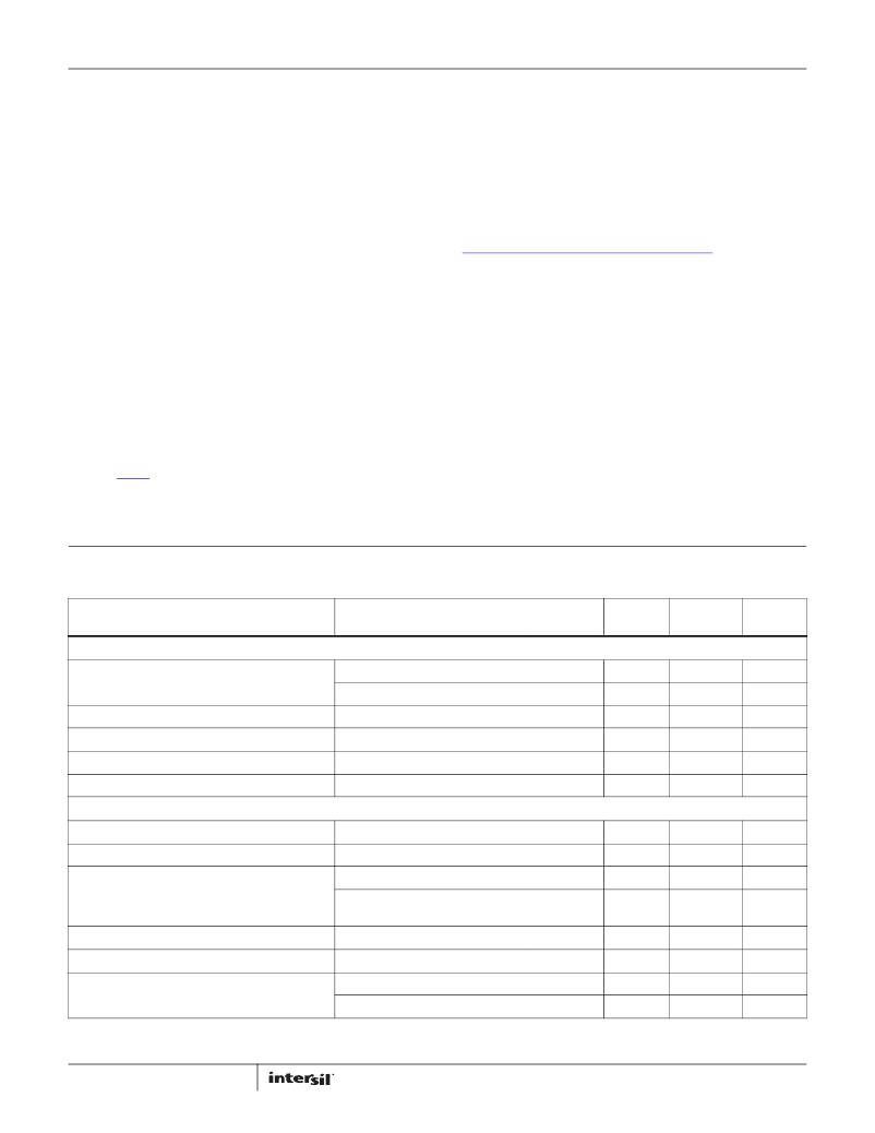
�Electrical� Specifications� V� DDP� =� V� DDS� =� 12V,� T� A� =� -40°C� to� +85°C� unless� otherwise� noted.� (Note� 8)� Typical� values� are� at� T� A� =� +25°C.�
�Boldface� limits� apply� over� the� operating� temperature� range,� -40°C� to� +85°C.�
�MIN�
�MAX�
�PARAMETER�
�CONDITIONS�
�(Note� 18)�
�TYP�
�(Note� 18)�
�UNIT�
�Input� and� Supply� Characteristics�
�I� DD� Supply� Current�
�I� DDS� Shutdown� Current�
�f� SW� =� 200kHz,� no� load�
�f� SW� =� 1MHz,� no� load�
�EN� =� 0V,� No� I� 2� C/SMBus� activity�
�11�
�15�
�0.6�
�20�
�30�
�1�
�mA�
�mA�
�mA�
�VR� Reference� Output� Voltage�
�VRA� Reference� Output� Voltage�
�V2P5� Reference� Output� Voltage�
�V� DD� >� 8V,� I� VR� <� 10mA�
�V� DD� >� 5.5V,� I� VRA� <� 20mA�
�I� V2P5� <� 20mA�
�6.5�
�4.5�
�2.25�
�7.0�
�5.1�
�2.5�
�7.5�
�5.5�
�2.75�
�V�
�V�
�V�
�Output� Characteristics�
�Output� Current�
�I� RMS� ,� Continuous�
�6�
�A�
�Output� Voltage� Adjustment� Range� (Note� 9)�
�Output� Voltage� Setpoint� Resolution�
�V� IN� >� V� OUT�
�Set� using� resistors�
�Set� using� I� 2� C/SMBus�
�0.6�
�10�
�±0.025�
�5.0�
�V�
�mV�
�%� FS�
�(Note� 10)�
�V� SEN� Output� Voltage� Accuracy�
�V� SEN� Input� Bias� Current�
�Soft-start� Delay� Duration� Range� (Note� 11)�
�Includes� line,� load,� temp�
�V� SEN� =� 5.5V�
�Set� using� SS� pin� or� resistor�
�-1�
�2�
�110�
�1�
�200�
�20�
�%�
�μA�
�ms�
�Set� using�
�I� 2� C/SMBus�
�0.002�
�500�
�s�
�6�
�FN6852.6�
�February� 20,� 2013�
�相关PDF资料 |
PDF描述 |
|---|---|
| R1D-3.33.3/P-R | CONV DC/DC 1W 3.3VIN +/-3.3VOUT |
| A9BBA-1802F | FLEX CABLE - AFF18A/AF18/AFF18A |
| 195D685X9025Y2T | CAP TANT 6.8UF 25V 10% 2910 |
| R1D-3.33.3/H-R | CONV DC/DC 1W 3.3VIN +/-3.3VOUT |
| 195D685X0025Y2T | CAP TANT 6.8UF 25V 20% 2910 |
相关代理商/技术参数 |
参数描述 |
|---|---|
| ZL212 | 制造商:SMC Corporation of America 功能描述:Multistage Ejector,Rc 1/8 Supply,Rc 3/4 |
| ZL212-DPL | 制造商:SMC Corporation of America 功能描述:VACUUM EJECTOR, W/O VALVE |
| ZL212-G | 制造商:SMC Corporation of America 功能描述:Vacuum Ejector; 1.2 mm x 2; 0.5 m; 200 per minute (AVR); 126 per minute (ANR) |
| ZL22B | 制造商:YEASHIN 制造商全称:YEASHIN 功能描述:500 mW DO-35 Hermetically Sealed Glass Zener Voltage Regulators |
| ZL24605 | 制造商:Microsemi Corporation 功能描述:5 OUTPUT ANY-RATE LINE CARD TIMING IC - Bulk |
发布紧急采购,3分钟左右您将得到回复。