参数资料
| 型号: | ZL6105ALAFTR5546 |
| 厂商: | Intersil |
| 文件页数: | 10/35页 |
| 文件大小: | 0K |
| 描述: | IC REG CTRLR BUCK PWM VM 36-QFN |
| 标准包装: | 100 |
| PWM 型: | 电压模式 |
| 输出数: | 1 |
| 频率 - 最大: | 1.4MHz |
| 占空比: | 95% |
| 电源电压: | 3 V ~ 14 V |
| 降压: | 是 |
| 升压: | 无 |
| 回扫: | 无 |
| 反相: | 无 |
| 倍增器: | 无 |
| 除法器: | 无 |
| Cuk: | 无 |
| 隔离: | 无 |
| 工作温度: | -40°C ~ 85°C |
| 封装/外壳: | 36-VFQFN 裸露焊盘 |
| 包装: | 托盘 |
第1页第2页第3页第4页第5页第6页第7页第8页第9页当前第10页第11页第12页第13页第14页第15页第16页第17页第18页第19页第20页第21页第22页第23页第24页第25页第26页第27页第28页第29页第30页第31页第32页第33页第34页第35页
�� �
�
�ZL6105�
�ZL6105� Overview�
�Digital-DC� Architecture�
�The� ZL6105� is� an� innovative� mixed-signal� power� conversion� and�
�power� management� IC� based� on� Zilker� Labs� patented� Digital-DC�
�technology� that� provides� an� integrated,� high� performance�
�Power� Conversion� Overview�
�The� ZL6105� operates� as� a� voltage-mode,� synchronous� buck�
�converter� with� a� selectable� constant� frequency� pulse� width�
�modulator� (PWM)� control� scheme� that� uses� external� MOSFETs,�
�capacitors,� and� an� inductor� to� perform� power� conversion.�
�V� IN�
�step-down� converter� for� a� wide� variety� of� power� supply�
�applications.�
�Today’s� embedded� power� systems� are� typically� designed� for� optimal�
�VR�
�BST�
�GH�
�DB�
�QH�
�C� IN�
�efficiency� at� maximum� load,� reducing� the� peak� thermal� stress� by�
�limiting� the� total� thermal� dissipation� inside� the� system.�
�Unfortunately,� many� of� these� systems� are� often� operated� at� load�
�ZL�
�SW�
�GL�
�CB�
�QL�
�V� OUT�
�C� OUT�
�levels� far� below� the� peak� where� the� power� system� has� been�
�optimized,� resulting� in� reduced� efficiency.� While� this� may� not� cause�
�thermal� stress� to� occur,� it� does� contribute� to� higher� electricity� usage�
�and� results� in� higher� overall� system� operating� costs.�
�Zilker� Labs’� efficiency-adaptive� ZL6105� DC/DC� controller� helps�
�mitigate� this� scenario� by� enabling� the� power� converter� to�
�automatically� change� their� operating� state� to� increase� efficiency�
�and� overall� performance� with� little� or� no� user� interaction� needed.�
�Auto� compensation� is� available� to� eliminate� the� need� for� manual�
�compensation� of� the� PID� filter.�
�Its� unique� PWM� loop� utilizes� an� ideal� mix� of� analog� and� digital�
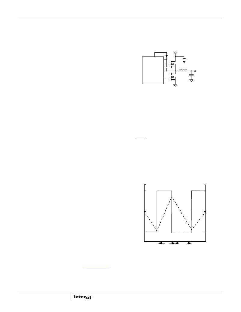
�FIGURE� 5.� SYNCHRONOUS� BUCK� CONVERTER�
�Figure� 5� illustrates� the� basic� synchronous� buck� converter�
�topology� showing� the� primary� power� train� components.� This�
�converter� is� also� called� a� step-down� converter,� as� the� output�
�voltage� must� always� be� lower� than� the� input� voltage.� In� its� most�
�simple� configuration,� the� ZL6105� requires� two� external�
�N-channel� power� MOSFETs,� one� for� the� top� control� MOSFET� (QH)�
�and� one� for� the� bottom� synchronous� MOSFET� (QL).� The� amount�
�of� time� that� QH� is� on� as� a� fraction� of� the� total� switching� period� is�
�known� as� the� duty� cycle� D� ,� which� is� described� by� Equation� 1:�
�blocks� to� enable� precise� control� of� the� entire� power� conversion�
�process� with� no� software� required,� resulting� in� a� very� flexible�
�device� that� is� also� very� easy� to� use.� An� extensive� set� of� power�
�D� ≈�
�V� OUT�
�V� IN�
�(EQ.� 1)�
�management� functions� are� fully� integrated� and� can� be�
�configured� using� simple� pin� connections.� The� user� configuration�
�can� be� saved� in� an� internal� non-volatile� memory� (NVM).�
�Additionally,� all� functions� can� be� configured� and� monitored� via�
�the� SMBus� hardware� interface� using� standard� PMBus�
�commands,� allowing� ultimate� flexibility.�
�Once� enabled,� the� ZL6105� is� immediately� ready� to� regulate�
�power� and� perform� power� management� tasks� with� no�
�During� time� D,� QH� is� on� and� V� IN� –� V� OUT� is� applied� across� the�
�inductor.� The� current� ramps� up� as� shown� in� Figure� 6.�
�When� QH� turns� off� (time� 1-D),� the� current� flowing� in� the� inductor�
�must� continue� to� flow� from� the� ground� up� through� QL,� during�
�which� the� current� ramps� down.� Since� the� output� capacitor� C� OUT�
�exhibits� a� low� impedance� at� the� switching� frequency,� the� AC�
�component� of� the� inductor� current� is� filtered� from� the� output�
�voltage� so� the� load� sees� nearly� a� DC� voltage.�
�programming� required.� Advanced� configuration� options� and�
�real-time� configuration� changes� are� available� via� the� I� 2� C/SMBus�
�interface� if� desired� and� continuous� monitoring� of� multiple�
�operating� parameters� is� possible� with� minimal� interaction� from� a�
�host� controller.� Integrated� sub-regulation� circuitry� enables� single�
�supply� operation� from� any� supply� between� 3V� and� 14V� with� no�
�secondary� bias� supplies� needed.�
�The� ZL6105� can� be� configured� by� simply� connecting� its� pins�
�according� to� the� tables� provided� in� the� following� sections.�
�Additionally,� a� comprehensive� set� of� development� tools� and�
�application� notes� are� available� to� help� simplify� the� design�
�process.� An� evaluation� board� is� also� available� to� help� the� user�
�become� familiar� with� the� device.� This� board� can� be� evaluated� as�
�a� standalone� platform� using� pin� configuration� settings.� A�
�V� IN� -� V� OUT�
�0�
�-V� OUT�
�D�
�1-D�
�IL� PK�
�I� O�
�IL� V�
�Windows?� based� GUI� is� also� provided� to� enable� full� configuration�
�and� monitoring� capability� via� the� I� 2� C/SMBus� interface� using� an�
�available� computer� and� the� included� USB� cable.�
�Application� notes� are� available� to� assist� the� user� in� designing� to�
�specific� application� demands.� Please� visit� www.intersil.com� to�
�access� the� most� up-to-date� documentation.�
�10�
�TIME�
�FIGURE� 6.� INDUCTOR� WAVEFORM�
�Typically,� buck� converters� specify� a� maximum� duty� cycle� that�
�effectively� limits� the� maximum� output� voltage� that� can� be� realized�
�for� a� given� input� voltage.� This� duty� cycle� limit� ensures� that� the�
�low-side� MOSFET� is� allowed� to� turn� on� for� a� minimum� amount� of�
�time� during� each� switching� cycle,� which� enables� the� bootstrap�
�capacitor� (CB� in� Figure� 6)� to� be� charged� up� and� provide� adequate�
�gate� drive� voltage� for� the� high-side� MOSFET.� See� “High-side� Driver�
�FN6906.5�
�December� 19,� 2013�
�相关PDF资料 |
PDF描述 |
|---|---|
| ZLDO1117G25TA | IC REG LDO 2.5V 1A SOT223-3 |
| ZLDO330T8TA | IC REG LDO 3.3V .3A SOT223-8 |
| ZLDO485T8TA | IC REG LDO 4.85V .3A SOT223-8 |
| ZLDO500T8TA | IC REG LDO 5V .3A SOT223-8 |
| ZM331643GTC | IC MONITOR 2.68V SUPPLY SOT223 |
相关代理商/技术参数 |
参数描述 |
|---|---|
| ZL62034UBJA | 制造商:TE Connectivity 功能描述:4x6.25 Gb/s TIA/LA Receiver D |
| ZL62B | 制造商:YEASHIN 制造商全称:YEASHIN 功能描述:500 mW DO-35 Hermetically Sealed Glass Zener Voltage Regulators |
| ZL68B | 制造商:YEASHIN 制造商全称:YEASHIN 功能描述:500 mW DO-35 Hermetically Sealed Glass Zener Voltage Regulators |
| ZL6V2B | 制造商:YEASHIN 制造商全称:YEASHIN 功能描述:500 mW DO-35 Hermetically Sealed Glass Zener Voltage Regulators |
| ZL6V8B | 制造商:YEASHIN 制造商全称:YEASHIN 功能描述:500 mW DO-35 Hermetically Sealed Glass Zener Voltage Regulators |
发布紧急采购,3分钟左右您将得到回复。