参数资料
| 型号: | ZL6105ALAFTR5546 |
| 厂商: | Intersil |
| 文件页数: | 7/35页 |
| 文件大小: | 0K |
| 描述: | IC REG CTRLR BUCK PWM VM 36-QFN |
| 标准包装: | 100 |
| PWM 型: | 电压模式 |
| 输出数: | 1 |
| 频率 - 最大: | 1.4MHz |
| 占空比: | 95% |
| 电源电压: | 3 V ~ 14 V |
| 降压: | 是 |
| 升压: | 无 |
| 回扫: | 无 |
| 反相: | 无 |
| 倍增器: | 无 |
| 除法器: | 无 |
| Cuk: | 无 |
| 隔离: | 无 |
| 工作温度: | -40°C ~ 85°C |
| 封装/外壳: | 36-VFQFN 裸露焊盘 |
| 包装: | 托盘 |
第1页第2页第3页第4页第5页第6页当前第7页第8页第9页第10页第11页第12页第13页第14页第15页第16页第17页第18页第19页第20页第21页第22页第23页第24页第25页第26页第27页第28页第29页第30页第31页第32页第33页第34页第35页
�� �
�
�ZL6105�
�Absolute� Maximum� Ratings� (Note� 7)�
�DC� Supply� Voltage� for� VDD� Pin� .� .� .� .� .� .� .� .� .� .� .� .� .� .� .� .� .� .� .� .� .� .� .� .� .� .� -0.3V� to� 17V�
�MOSFET� Drive� Reference� for� VR� Pin� @� 120mA� .� .� .� .� .� .� .� .� .� .� .� -0.3V� to� 6.5V�
�2.5V� Logic� Reference� for� V25� Pin� @� 120mA� .� .� .� .� .� .� .� .� .� .� .� .� .� .� .� -0.3V� to� 3V�
�Logic� I/O� Voltage� for� CFG(0,1,2),� DDC,� EN,�
�FC(0,� 1),� ILIM,� MGN,� PG,� PH_EN,� SA(0,� 1),� SALRT,�
�SCL,� SDA,� SS,� SYNC,� UVLO,� V(0,1)� Pins� .� .� .� .� .� .� .� .� .� .� .� .� .� .� .� .� -0.3V� to� 6.5V�
�Analog� Input� Voltages� for� ISENB,� VSEN,� VTRK,�
�XTEMP� Pins� .� .� .� .� .� .� .� .� .� .� .� .� .� .� .� .� .� .� .� .� .� .� .� .� .� .� .� .� .� .� .� .� .� .� .� .� .� .� .� -0.3V� to� 6.5V�
�Analog� Input� Voltages� for� ISENA� Pin� .� .� .� .� .� .� .� .� .� .� .� .� .� .� .� .� .� .� .� .� .� -1.5V� to� 30V�
�High� Side� Supply� Voltage� for� BST� Pin� .� .� .� .� .� .� .� .� .� .� .� .� .� .� .� .� .� .� .� .� -0.3V� to� 30V�
�Boost� to� Switch� Voltage� for� BST� -� SW� Pins� .� .� .� .� .� .� .� .� .� .� .� .� .� .� .� .� .� -0.3V� to� 8V�
�High� Side� Drive� Voltage� for� GH� Pin�
�.� .� .� .� .� .� .� .� .� .� .� .� .� .� .� .� .� .� .� .� .� .� .� .� .� .� .� .� .� .� .� .� .� .� .� .� .(V� SW� -� 0.3V)� to� (V� BST� +� 0.3V)�
�Low� Side� Drive� Voltage� for� GL� Pin� .� .� .� .� .� .� .� .� .� .� (PGND� -� 0.3V)� to� VR� +� 0.3V�
�Switch� Node� for� SW� Pin�
�Continuous� .� .� .� .� .� .� .� .� .� .� .� .� .� .� .� .� .� .� .� .� .� .� .� .� .� .� .� .� .� .� .� .� .(PGND� -� 0.3V)� to� 30V�
�Thermal� Information�
�Thermal� Resistance� (Typical)� θ� JA� (°C/W)� θ� JC� (°C/W)�
�36� Ld� QFN� (Notes� 9,� 10)� .� .� .� .� .� .� .� .� .� .� .� .� .� .� .� 35� 5�
�Operating� Junction� Temperature� Range� .� .� .� .� .� .� .� .� .� .� .� .� .� .-40°C� to� +125°C�
�Junction� Temperature� .� .� .� .� .� .� .� .� .� .� .� .� .� .� .� .� .� .� .� .� .� .� .� .� .� .� .� .� .� .-55°C� to� +150°C�
�Storage� Temperature� Range.� .� .� .� .� .� .� .� .� .� .� .� .� .� .� .� .� .� .� .� .� .� .� .-55°C� to� +150°C�
�Pb-Free� Reflow� Profile� .� .� .� .� .� .� .� .� .� .� .� .� .� .� .� .� .� .� .� .� .� .� .� .� .� .� .� .� .� .� .� see� link� below�
��Recommended� Operating� Conditions�
�Input� Supply� Voltage� Range,� V� DD� (see� Figure� 8)�
�V� DD� tied� to� V� R� .� .� .� .� .� .� .� .� .� .� .� .� .� .� .� .� .� .� .� .� .� .� .� .� .� .� .� .� .� .� .� .� .� .� .� .� .� .� .� 3.0V� to� 5V�
�V� R� floating� .� .� .� .� .� .� .� .� .� .� .� .� .� .� .� .� .� .� .� .� .� .� .� .� .� .� .� .� .� .� .� .� .� .� .� .� .� .� .� .� .� 4.5V� to� 14V�
�Output� Voltage� Range� (V� OUT� )� (Note� 11)� .� .� .� .� .� .� .� .� .� .� .� .� .� .� .� .� .� .� 0.54V� to� 5.5V�
�Junction� Temperature� .� .� .� .� .� .� .� .� .� .� .� .� .� .� .� .� .� .� .� .� .� .� .� .� .� .� .� .� .� .-40°C� to� +125°C�
�Transient� (<100ns)� .� .� .� .� .� .� .� .� .� .� .� .� .� .� .� .� .� .� .� .� .� .� .� .� .� .� .� .� (PGND� -� 5V)� to� 30V�
�Ground� Voltage� Differential� (� DGND� -� SGND,� PGND� -� SGND� )�
�for� DGND,� SGND� and� PGND� Pins� .� .� .� .� .� .� .� .� .� .� .� .� .� .� .� .� .� .� .� .� -0.3V� to� +0.3V�
�ESD� Rating�
�Human� Body� Model� (Note� 8).� .� .� .� .� .� .� .� .� .� .� .� .� .� .� .� .� .� .� .� .� .� .� .� .� .� .� .� .� .� .� .� .� 2kV�
�Machine� Model� .� .� .� .� .� .� .� .� .� .� .� .� .� .� .� .� .� .� .� .� .� .� .� .� .� .� .� .� .� .� .� .� .� .� .� .� .� .� .� .� .� .� 500V�
�Latch-up� .� .� .� .� .� .� .� .� .� .� .� .� .� .� .� .� .� .� .� .� .� .� .� .� .� .� .� .� .� .� .� .� .� .� .� .� .� .� .� .� .Tested� to� JESD78�
�CAUTION:� Do� not� operate� at� or� near� the� maximum� ratings� listed� for� extended� periods� of� time.� Exposure� to� such� conditions� may� adversely� impact� product�
�reliability� and� result� in� failures� not� covered� by� warranty.�
�NOTES:�
�7.� Voltage� measured� with� respect� to� SGND.�
�8.� BST,� SW� pins� rated� at� 1.5kV.�
�9.� θ� JA� is� measured� in� free� air� with� the� component� mounted� on� a� high� effective� thermal� conductivity� test� board� with� “direct� attach”� features.� See� Tech�
�Brief� TB379.�
�10.� For� θ� JC� ,� the� “case� temp”� location� is� the� center� of� the� exposed� metal� pad� on� the� package� underside.�
�11.� Includes� margin� limits.�
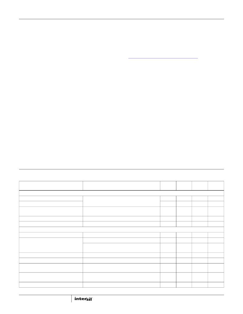
�Electrical� Specifications� V� DD� =� 12V,� T� A� =� -40°C� to� +85°C� unless� otherwise� noted.� Typical� values� are� at� T� A� =� +25°C.� Boldface� limits� apply� over�
�the� operating� temperature� range,� -40°C� to� +85°C.�
�MIN�
�MAX�
�PARAMETER�
�CONDITIONS�
�(Note� 19)�
�TYP�
�(Note� 19)�
�UNIT�
�Input� and� Supply� Characteristics�
�I� DD� Supply� Current� at� f� SW� =� 200kHz�
�I� DD� Supply� Current� at� f� SW� =� 1.4Mhz�
�I� DDS� Shutdown� Current�
�Vr� Reference� Output� Voltage�
�V25� Reference� Output� Voltage�
�GH,� GL� no� load�
�EN� =� 0V�
�No� I� 2� C/SMBus� activity�
�V� DD� >� 6V,� I� VR� <� 20mA�
�V� R� >� 3V,� I� V25� <� 20mA�
�–�
�–�
�–�
�4.5�
�2.25�
�16�
�25�
�6.5�
�5.2�
�2.5�
�30�
�50�
�9�
�5.5�
�2.75�
�mA�
�mA�
�mA�
�V�
�V�
�Output� Characteristics�
�Output� Voltage� Adjustment� Range� (Note� 12)�
�Output� Voltage� Set-point� Resolution�
�V� IN� >� V� OUT�
�Set� using� resistors�
�Set� using� I� 2� C/SMBus�
�0.6�
�–�
�–�
�–�
�10�
�±0.025�
�5.0�
�–�
�–�
�V�
�mV�
�%� FS�
�(Note� 13)�
�Output� Voltage� Accuracy� (Note� 14)�
�Vsen� Input� Bias� Current�
�Current� Sense� Differential� Input�
�Voltage� (Ground� Referenced)�
�Current� Sense� Differential� Input� Voltage� (V� out�
�Referenced,� V� out� <� 4.0V)�
�Current� Sense� Input� Bias� Current�
�Includes� line,� load,� temp�
�VSEN� =� 5.5V�
�V� ISENA� -V� ISENB�
�V� ISENA� -V� ISENB�
�Ground� referenced�
�-1�
�–�
�-100�
�-50�
�-100�
�–�
�110�
�–�
�–�
�–�
�1�
�200�
�100�
�50�
�100�
�%�
�μA�
�mV�
�mV�
�μA�
�7�
�FN6906.5�
�December� 19,� 2013�
�相关PDF资料 |
PDF描述 |
|---|---|
| ZLDO1117G25TA | IC REG LDO 2.5V 1A SOT223-3 |
| ZLDO330T8TA | IC REG LDO 3.3V .3A SOT223-8 |
| ZLDO485T8TA | IC REG LDO 4.85V .3A SOT223-8 |
| ZLDO500T8TA | IC REG LDO 5V .3A SOT223-8 |
| ZM331643GTC | IC MONITOR 2.68V SUPPLY SOT223 |
相关代理商/技术参数 |
参数描述 |
|---|---|
| ZL62034UBJA | 制造商:TE Connectivity 功能描述:4x6.25 Gb/s TIA/LA Receiver D |
| ZL62B | 制造商:YEASHIN 制造商全称:YEASHIN 功能描述:500 mW DO-35 Hermetically Sealed Glass Zener Voltage Regulators |
| ZL68B | 制造商:YEASHIN 制造商全称:YEASHIN 功能描述:500 mW DO-35 Hermetically Sealed Glass Zener Voltage Regulators |
| ZL6V2B | 制造商:YEASHIN 制造商全称:YEASHIN 功能描述:500 mW DO-35 Hermetically Sealed Glass Zener Voltage Regulators |
| ZL6V8B | 制造商:YEASHIN 制造商全称:YEASHIN 功能描述:500 mW DO-35 Hermetically Sealed Glass Zener Voltage Regulators |
发布紧急采购,3分钟左右您将得到回复。