参数资料
| 型号: | ZL6105ALAFTR5546 |
| 厂商: | Intersil |
| 文件页数: | 11/35页 |
| 文件大小: | 0K |
| 描述: | IC REG CTRLR BUCK PWM VM 36-QFN |
| 标准包装: | 100 |
| PWM 型: | 电压模式 |
| 输出数: | 1 |
| 频率 - 最大: | 1.4MHz |
| 占空比: | 95% |
| 电源电压: | 3 V ~ 14 V |
| 降压: | 是 |
| 升压: | 无 |
| 回扫: | 无 |
| 反相: | 无 |
| 倍增器: | 无 |
| 除法器: | 无 |
| Cuk: | 无 |
| 隔离: | 无 |
| 工作温度: | -40°C ~ 85°C |
| 封装/外壳: | 36-VFQFN 裸露焊盘 |
| 包装: | 托盘 |
第1页第2页第3页第4页第5页第6页第7页第8页第9页第10页当前第11页第12页第13页第14页第15页第16页第17页第18页第19页第20页第21页第22页第23页第24页第25页第26页第27页第28页第29页第30页第31页第32页第33页第34页第35页
�� �
�
�ZL6105�
��In� general,� the� size� of� components� L1� and� C� OUT� as� well� as� the�
�overall� efficiency� of� the� circuit� are� inversely� proportional� to� the�
�switching� frequency,� f� SW� .� Therefore,� the� highest� efficiency� circuit�
�may� be� realized� by� switching� the� MOSFETs� at� the� lowest� possible�
�frequency;� however,� this� will� result� in� the� largest� component� size.�
�Conversely,� the� smallest� possible� footprint� may� be� realized� by�
�switching� at� the� fastest� possible� frequency� but� this� gives� a�
�somewhat� lower� efficiency.� Each� user� should� determine� the�
�optimal� combination� of� size� and� efficiency� when� determining� the�
�switching� frequency� for� each� application.�
�The� block� diagram� for� the� ZL6105� is� illustrated� in� Figure� 4.� In� this�
�circuit,� the� target� output� voltage� is� regulated� by� connecting� the�
�differential� VSEN� pins� directly� to� the� output� regulation� point.� The�
�VSEN� signal� is� then� compared� to� a� reference� voltage� that� has�
�been� set� to� the� desired� output� voltage� level� by� the� user.� The� error�
�signal� derived� from� this� comparison� is� converted� to� a� digital�
�value� with� a� low-resolution,� analog� to� digital� (A/D)� converter.� The�
�digital� signal� is� applied� to� an� adjustable� digital� compensation�
�filter,� and� the� compensated� signal� is� used� to� derive� the�
�appropriate� PWM� duty� cycle� for� driving� the� external� MOSFETs� in� a�
�PIN-STRAP� SETTINGS�
�This� is� the� simplest� implementation� method,� as� no� external�
�components� are� required.� Using� this� method,� each� pin� can� take�
�on� one� of� three� possible� states:� LOW,� OPEN,� or� HIGH.� These� pins�
�can� be� connected� to� the� V25� pin� for� logic� HIGH� settings� as� this�
�pin� provides� a� regulated� voltage� higher� than� 2V.� Using� a� single�
�pin,� one� of� three� settings� can� be� selected.� Using� two� pins,� one� of�
�nine� settings� can� be� selected.�
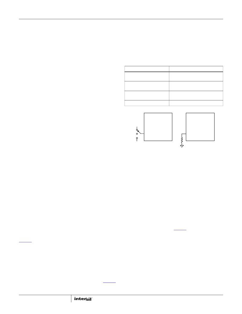
�TABLE� 1.� MULTI-MODE� PIN� CONFIGURATION�
�PIN� TIED� TO� VALUE�
�LOW� <� 0.8� VDC�
�(Logic� LOW)�
�OPEN� No� connection�
�(N/C)�
�HIGH� >� 2.0� VDC�
�(Logic� HIGH)�
�Resistor� to� SGND� Set� by� resistor� value�
�way� that� produces� the� desired� output.�
�The� ZL6105� has� several� features� to� improve� the� power�
�conversion� efficiency.� A� non-linear� response� (NLR)� loop� improves�
�the� response� time� and� reduces� the� output� deviation� as� a� result� of�
�Logic�
�high�
�Open�
�ZL�
�Multi-� mode� Pin�
�ZL�
�Multi-� mode� Pin�
�a� load� transient.� The� ZL6105� monitors� the� power� converter’s�
�operating� conditions� and� continuously� adjusts� the� turn-on� and�
�Logic�
�low�
�Pin-strap�
�R� SET�
�Resistor�
�turn-off� timing� of� the� high-side� and� low-side� MOSFETs� to� optimize�
�the� overall� efficiency� of� the� power� supply.� Adaptive� performance�
�optimization� algorithms� such� as� dead-time� control,� diode�
�emulation,� and� frequency� control� are� available� to� provide� greater�
�efficiency� improvement.�
�Power� Management� Overview�
�The� ZL6105� incorporates� a� wide� range� of� configurable� power�
�management� features� that� are� simple� to� implement� with� no�
�external� components.� Additionally,� the� ZL6105� includes� circuit�
�protection� features� that� continuously� safeguard� the� device� and�
�load� from� damage� due� to� unexpected� system� faults.� The� ZL6105�
�can� continuously� monitor� input� voltage,� output� voltage/current,�
�internal� temperature,� and� the� temperature� of� an� external�
�thermal� diode.� A� Power-Good� output� signal� is� also� included� to�
�enable� power-on� reset� functionality� for� an� external� processor.�
�All� power� management� functions� can� be� configured� using� either�
�pin� configuration� techniques� (see� Figure� 8)� or� via� the� I� 2� C/SMBus�
�interface.� Monitoring� parameters� can� also� be� pre-configured� to�
�provide� alerts� for� specific� conditions.� See� Application� Note�
�AN2033� for� more� details� on� SMBus� monitoring.�
�Multi-mode� Pins�
�In� order� to� simplify� circuit� design,� the� ZL6105� incorporates� patented�
�multi-mode� pins� that� allow� the� user� to� easily� configure� many�
�aspects� of� the� device� with� no� programming.� Most� power�
�management� features� can� be� configured� using� these� pins.� The�
�multi-mode� pins� can� respond� to� four� different� connections� as� shown�
�in� Table� 1.� These� pins� are� sampled� when� power� is� applied� or� by�
�issuing� a� PMBus� Restore� command� (see� Application� Note� AN2033� ).�
�11�
�Settings� Settings�
�FIGURE� 7.� PIN-STRAP� AND� RESISTOR� SETTING� EXAMPLES�
�RESISTOR� SETTINGS�
�This� method� allows� a� greater� range� of� adjustability� when� connecting�
�a� finite� value� resistor� (in� a� specified� range)� between� the� multi-mode�
�pin� and� SGND.� Standard� 1%� resistor� values� are� used,� and� only� every�
�fourth� E96� resistor� value� is� used� so� the� device� can� reliably� recognize�
�the� value� of� resistance� connected� to� the� pin� while� eliminating� the�
�error� associated� with� the� resistor� accuracy.� Up� to� 31� unique�
�selections� are� available� using� a� single� resistor.�
�I� 2� C/SMBUS� METHOD�
�Almost� any� ZL6105� function� can� be� configured� via� the� I� 2� C/SMBus�
�interface� using� standard� PMBus� commands.� Additionally,� any� value�
�that� has� been� configured� using� the� pin-strap� or� resistor� setting�
�methods� can� also� be� re-configured� and/or� verified� via� the�
�I� 2� C/SMBus.� See� Application� Note� AN2033� for� more� details.�
�The� SMBus� device� address� and� VOUT_MAX� are� the� only�
�parameters� that� must� be� set� by� external� pins.� All� other� device�
�parameters� can� be� set� via� the� I� 2� C/SMBus.� The� device� address� is�
�set� using� the� SA0� and� SA1� pins.� VOUT_MAX� is� determined� as�
�10%� greater� than� the� voltage� set� by� the� V0� and� V1� pins.�
�FN6906.5�
�December� 19,� 2013�
�相关PDF资料 |
PDF描述 |
|---|---|
| ZLDO1117G25TA | IC REG LDO 2.5V 1A SOT223-3 |
| ZLDO330T8TA | IC REG LDO 3.3V .3A SOT223-8 |
| ZLDO485T8TA | IC REG LDO 4.85V .3A SOT223-8 |
| ZLDO500T8TA | IC REG LDO 5V .3A SOT223-8 |
| ZM331643GTC | IC MONITOR 2.68V SUPPLY SOT223 |
相关代理商/技术参数 |
参数描述 |
|---|---|
| ZL62034UBJA | 制造商:TE Connectivity 功能描述:4x6.25 Gb/s TIA/LA Receiver D |
| ZL62B | 制造商:YEASHIN 制造商全称:YEASHIN 功能描述:500 mW DO-35 Hermetically Sealed Glass Zener Voltage Regulators |
| ZL68B | 制造商:YEASHIN 制造商全称:YEASHIN 功能描述:500 mW DO-35 Hermetically Sealed Glass Zener Voltage Regulators |
| ZL6V2B | 制造商:YEASHIN 制造商全称:YEASHIN 功能描述:500 mW DO-35 Hermetically Sealed Glass Zener Voltage Regulators |
| ZL6V8B | 制造商:YEASHIN 制造商全称:YEASHIN 功能描述:500 mW DO-35 Hermetically Sealed Glass Zener Voltage Regulators |
发布紧急采购,3分钟左右您将得到回复。