参数资料
| 型号: | A3P600-FG484 |
| 厂商: | Microsemi SoC |
| 文件页数: | 1/220页 |
| 文件大小: | 0K |
| 描述: | IC FPGA 1KB FLASH 600K 484-FBGA |
| 标准包装: | 40 |
| 系列: | ProASIC3 |
| RAM 位总计: | 110592 |
| 输入/输出数: | 235 |
| 门数: | 600000 |
| 电源电压: | 1.425 V ~ 1.575 V |
| 安装类型: | 表面贴装 |
| 工作温度: | 0°C ~ 70°C |
| 封装/外壳: | 484-BGA |
| 供应商设备封装: | 484-FPBGA(23x23) |
当前第1页第2页第3页第4页第5页第6页第7页第8页第9页第10页第11页第12页第13页第14页第15页第16页第17页第18页第19页第20页第21页第22页第23页第24页第25页第26页第27页第28页第29页第30页第31页第32页第33页第34页第35页第36页第37页第38页第39页第40页第41页第42页第43页第44页第45页第46页第47页第48页第49页第50页第51页第52页第53页第54页第55页第56页第57页第58页第59页第60页第61页第62页第63页第64页第65页第66页第67页第68页第69页第70页第71页第72页第73页第74页第75页第76页第77页第78页第79页第80页第81页第82页第83页第84页第85页第86页第87页第88页第89页第90页第91页第92页第93页第94页第95页第96页第97页第98页第99页第100页第101页第102页第103页第104页第105页第106页第107页第108页第109页第110页第111页第112页第113页第114页第115页第116页第117页第118页第119页第120页第121页第122页第123页第124页第125页第126页第127页第128页第129页第130页第131页第132页第133页第134页第135页第136页第137页第138页第139页第140页第141页第142页第143页第144页第145页第146页第147页第148页第149页第150页第151页第152页第153页第154页第155页第156页第157页第158页第159页第160页第161页第162页第163页第164页第165页第166页第167页第168页第169页第170页第171页第172页第173页第174页第175页第176页第177页第178页第179页第180页第181页第182页第183页第184页第185页第186页第187页第188页第189页第190页第191页第192页第193页第194页第195页第196页第197页第198页第199页第200页第201页第202页第203页第204页第205页第206页第207页第208页第209页第210页第211页第212页第213页第214页第215页第216页第217页第218页第219页第220页
January 2013
I
2013 Microsemi Corporation
ProASIC3 Flash Family FPGAs
with Optional Soft ARM Support
Features and Benefits
High Capacity
15 k to 1 M System Gates
Up to 144 kbits of True Dual-Port SRAM
Up to 300 User I/Os
Reprogrammable Flash Technology
130-nm, 7-Layer Metal (6 Copper), Flash-Based CMOS
Process
Instant On Level 0 Support
Single-Chip Solution
Retains Programmed Design when Powered Off
High Performance
350 MHz System Performance
3.3 V, 66 MHz 64-Bit PCI
In-System Programming (ISP) and Security
ISP Using On-Chip 128-Bit Advanced Encryption Standard
(AES) Decryption (except ARM-enabled ProASIC3 devices)
via JTAG (IEEE 1532–compliant)
FlashLock to Secure FPGA Contents
Low Power
Core Voltage for Low Power
Support for 1.5 V-Only Systems
Low-Impedance Flash Switches
High-Performance Routing Hierarchy
Segmented, Hierarchical Routing and Clock Structure
Advanced I/O
700 Mbps DDR, LVDS-Capable I/Os (A3P250 and above)
1.5 V, 1.8 V, 2.5 V, and 3.3 V Mixed-Voltage Operation
Wide Range Power Supply Voltage Support per JESD8-B,
Allowing I/Os to Operate from 2.7 V to 3.6 V
Bank-Selectable I/O Voltages—up to 4 Banks per Chip
Single-Ended
I/O
Standards:
LVTTL,
LVCMOS
3.3 V /
2.5 V / 1.8 V / 1.5 V, 3.3 V PCI / 3.3 V PCI-X and LVCMOS
2.5 V / 5.0 V Input
Differential I/O Standards: LVPECL, LVDS, B-LVDS, and
M-LVDS (A3P250 and above)
I/O Registers on Input, Output, and Enable Paths
Hot-Swappable and Cold Sparing I/Os
Weak Pull-Up/-Down
IEEE 1149.1 (JTAG) Boundary Scan Test
Pin-Compatible Packages across the ProASIC3 Family
Clock Conditioning Circuit (CCC) and PLL
Six CCC Blocks, One with an Integrated PLL
Configurable Phase-Shift, Multiply/Divide, Delay Capabilities
and External Feedback
Wide Input Frequency Range (1.5 MHz to 350 MHz)
1 kbit of FlashROM User Nonvolatile Memory
SRAMs and FIFOs with Variable-Aspect-Ratio 4,608-Bit RAM
True Dual-Port SRAM (except ×18)
ARM Processor Support in ProASIC3 FPGAs
M1 ProASIC3 Devices—ARMCortex-M1 Soft Processor
Available with or without Debug
A3P015 and A3P030 devices do not support this feature.
Supported only by A3P015 and A3P030 devices.
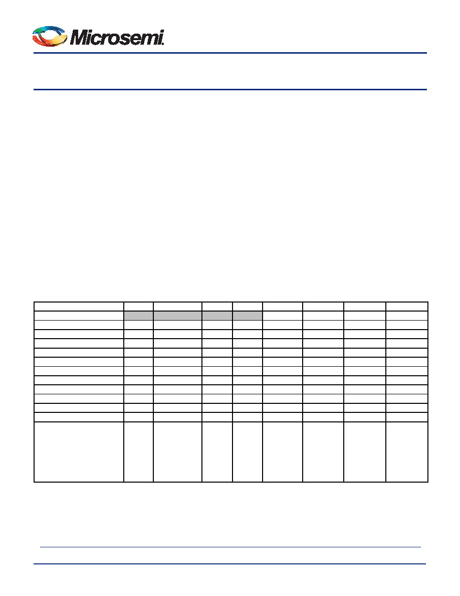
ProASIC3 Devices
A3P0151
A3P030
A3P060
A3P125
A3P250
A3P400
A3P600
A3P1000
Cortex-M1 Devices 2
M1A3P250
M1A3P400
M1A3P600
M1A3P1000
System Gates
15,000
30,000
60,000
125,000
250,000
400,000
600,000
1,000,000
Typical Equivalent Macrocells
128
256
512
1,024
2,048
–
VersaTiles (D-flip-flops)
384
768
1,536
3,072
6,144
9,216
13,824
24,576
RAM Kbits (1,024 bits)
–
18
36
54
108
144
4,608-Bit Blocks
––
4
8
12
24
32
FlashROM Kbits
11
1
Secure (AES) ISP 3
–
Yes
Integrated PLL in CCCs
––
1
VersaNet Globals 4
6
18
I/O Banks
22
2
4
Maximum User I/Os
49
81
96
133
157
194
235
300
Package Pins
QFN
CS
VQFP
TQFP
PQFP
FBGA
QN68
QN48, QN68,
QN132
VQ100
QN132
CS121
VQ100
TQ144
FG144
QN132
VQ100
TQ144
PQ208
FG144
QN132 5
VQ100
PQ208
FG144/256 5
PQ208
FG144/256/
484
PQ208
FG144/256/
484
PQ208
FG144/256/
484
Notes:
1. A3P015 is not recommended for new designs.
2. Refer to the Cortex-M1 product brief for more information.
3. AES is not available for Cortex-M1 ProASIC3 devices.
4. Six chip (main) and three quadrant global networks are available for A3P060 and above.
5. The M1A3P250 device does not support this package.
6. For higher densities and support of additional features, refer to the ProASIC3E Flash Family FPGAs datasheet.
Revision 13
相关PDF资料 |
PDF描述 |
|---|---|
| M1A3P600-FGG484 | IC FPGA 1KB FLASH 600K 484-FBGA |
| M1A3P600-FG484 | IC FPGA 1KB FLASH 600K 484-FBGA |
| EX256-PTQ100 | IC FPGA ANTIFUSE 12K 100-TQFP |
| EX256-PTQG100 | IC FPGA ANTIFUSE 12K 100-TQFP |
| A54SX08A-PQ208A | IC FPGA SX 12K GATES 208-PQFP |
相关代理商/技术参数 |
参数描述 |
|---|---|
| A3P600-FG484I | 功能描述:IC FPGA 1KB FLASH 600K 484-FBGA RoHS:否 类别:集成电路 (IC) >> 嵌入式 - FPGA(现场可编程门阵列) 系列:ProASIC3 标准包装:40 系列:SX-A LAB/CLB数:6036 逻辑元件/单元数:- RAM 位总计:- 输入/输出数:360 门数:108000 电源电压:2.25 V ~ 5.25 V 安装类型:表面贴装 工作温度:0°C ~ 70°C 封装/外壳:484-BGA 供应商设备封装:484-FPBGA(27X27) |
| A3P600-FGG144 | 功能描述:IC FPGA 235I/O 144FBGA RoHS:是 类别:集成电路 (IC) >> 嵌入式 - FPGA(现场可编程门阵列) 系列:ProASIC3 标准包装:60 系列:XP LAB/CLB数:- 逻辑元件/单元数:10000 RAM 位总计:221184 输入/输出数:244 门数:- 电源电压:1.71 V ~ 3.465 V 安装类型:表面贴装 工作温度:0°C ~ 85°C 封装/外壳:388-BBGA 供应商设备封装:388-FPBGA(23x23) 其它名称:220-1241 |
| A3P600-FGG144ES | 制造商:ACTEL 制造商全称:Actel Corporation 功能描述:ProASIC3 Flash Family FPGAs |
| A3P600-FGG144I | 功能描述:IC FPGA 1KB FLASH 600K 144-FBGA RoHS:是 类别:集成电路 (IC) >> 嵌入式 - FPGA(现场可编程门阵列) 系列:ProASIC3 标准包装:90 系列:ProASIC3 LAB/CLB数:- 逻辑元件/单元数:- RAM 位总计:36864 输入/输出数:157 门数:250000 电源电压:1.425 V ~ 1.575 V 安装类型:表面贴装 工作温度:-40°C ~ 125°C 封装/外壳:256-LBGA 供应商设备封装:256-FPBGA(17x17) |
| A3P600-FGG144PP | 制造商:ACTEL 制造商全称:Actel Corporation 功能描述:ProASIC3 Flash Family FPGAs |
发布紧急采购,3分钟左右您将得到回复。