- 您现在的位置:买卖IC网 > PDF目录298744 > A42MX24-3VQ100A (Electronic Theatre Controls, Inc.) 40MX and 42MX FPGA Families PDF资料下载
参数资料
| 型号: | A42MX24-3VQ100A |
| 厂商: | Electronic Theatre Controls, Inc. |
| 英文描述: | 40MX and 42MX FPGA Families |
| 中文描述: | 40MX和42MX FPGA系列 |
| 文件页数: | 37/93页 |
| 文件大小: | 854K |
| 代理商: | A42MX24-3VQ100A |
第1页第2页第3页第4页第5页第6页第7页第8页第9页第10页第11页第12页第13页第14页第15页第16页第17页第18页第19页第20页第21页第22页第23页第24页第25页第26页第27页第28页第29页第30页第31页第32页第33页第34页第35页第36页当前第37页第38页第39页第40页第41页第42页第43页第44页第45页第46页第47页第48页第49页第50页第51页第52页第53页第54页第55页第56页第57页第58页第59页第60页第61页第62页第63页第64页第65页第66页第67页第68页第69页第70页第71页第72页第73页第74页第75页第76页第77页第78页第79页第80页第81页第82页第83页第84页第85页第86页第87页第88页第89页第90页第91页第92页第93页
42
Data Device Corporation
www.ddc-web.com
BU-6474X/6484X/6486X
J-07/05-0
CLOCK IN
t1
t6
t7
t2
t3
t18
t16
VALID
t8
t9
t14
t15
t17
VALID
t12
t10
t4
t11
t5
VALID
t13
SELECT
(Note 2,7)
(Note 2)
(Note 3,4,7)
(Note 4,5)
STRBD
MEM/REG
RD/WR
IOEN
(Note 2,6)
(Note 6)
(Note 9,10)
(Note 7,8,9,10)
READYD
A15-A0
D15-D0
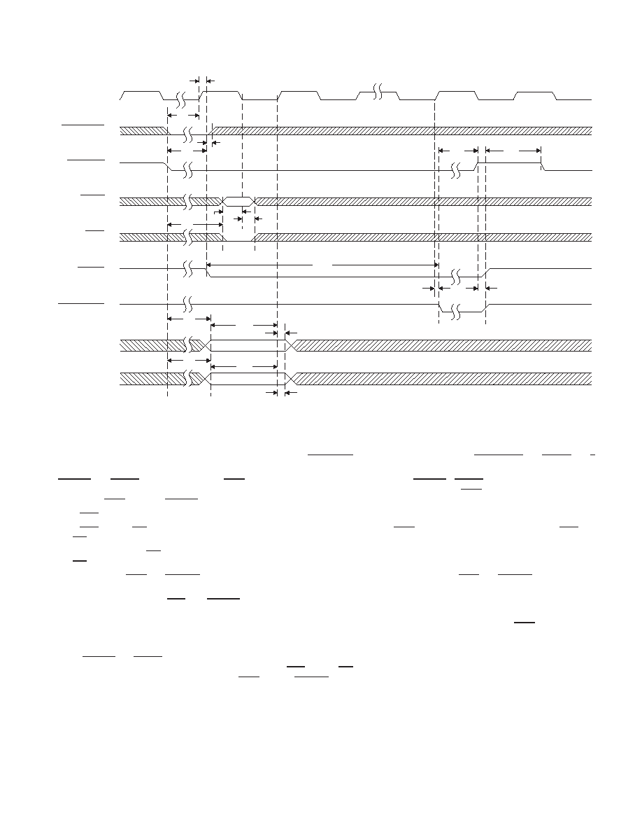
FIGURE 14. CPU WRITING RAM / REGISTER (16-BIT BUFFERED, NONZERO WAIT)
NOTES:
1.
For the 16-bit buffered nonzero wait configuration TRANSPARENT/BUFFERED must be connected to logic "0", ZERO_WAIT and DTREG / 16/8
must be connected to logic "1". The inputs TRIGGER_SEL and MSB/LSB may be connected to either Vcc or ground.
2.
SELECT and STRBD may be tied together. IOEN goes low on the first rising CLK edge when SELECT STRBD is sampled low (satisfying t1)
and the Mark3’s protocol/memory management logic is not accessing the internal RAM. When this occurs, IOEN goes low, starting the transfer
cycle. After IOEN goes low, SELECT may be released high.
3.
MEM/REG must be presented high for memory access, low for register access.
4.
MEM/REG and RD/WR are buffered transparently until the first falling edge of CLK after IOEN goes low. After this CLK edge, MEM/REG and
RD/WR become latched internally.
5.
The logic sense for RD/WR in the diagram assumes that POLARITY_SEL is connected to logic "1". If POLARITY_SEL is connected to logic "0",
RD/WR must be asserted high to write.
6.
The timing for the IOEN and READYD outputs assume a 50 pf load. For loading above 50 pf, the validity of IOEN and READYD is delayed by an
additional 0.14 ns/pf typ, 0.28 ns/pf max.
7.
The timing for A15-A0, MEM/REG, and SELECT assumes that ADDR-LAT is connected to logic "1". Refer to Address Latch timing for additional
details.
8.
The address bus A15-A0 and data bus D15-D0 are internally buffered transparently until the first rising edge of CLK after IOEN goes low. After
this CLK edge, A15-A0 and D15-D0 become latched internally.
9.
Setup time given for use in worst case timing calculations. None of the Mark3’s input signals are required to be synchronized to the system clock.
When SELECT and STRBD do not meet the setup time of t1, but occur during the setup time of an internal flip-flop, an additional clock cycle may
be inserted between the falling clock edge that latches MEM/REG and RD/WR and the rising clock edge that latches the address (A15-A0) and
data (D15-D0). When this occurs, the delay from IOEN falling to READYD falling (t14) increases by one clock cycle and the address and data hold
time (t12 and t13) must be increased by one clock.
相关PDF资料 |
PDF描述 |
|---|---|
| A42MX24-3VQ100B | 40MX and 42MX FPGA Families |
| A42MX36-2PQ100B | 40MX and 42MX FPGA Families |
| A42MX36-2PQ100ES | 40MX and 42MX FPGA Families |
| A42MX36-2TQ100 | 40MX and 42MX FPGA Families |
| A42MX36-2TQ100A | 40MX and 42MX FPGA Families |
相关代理商/技术参数 |
参数描述 |
|---|---|
| A42MX24-FPL84 | 功能描述:IC FPGA MX SGL CHIP 36K 84-PLCC RoHS:否 类别:集成电路 (IC) >> 嵌入式 - FPGA(现场可编程门阵列) 系列:MX 标准包装:40 系列:SX-A LAB/CLB数:6036 逻辑元件/单元数:- RAM 位总计:- 输入/输出数:360 门数:108000 电源电压:2.25 V ~ 5.25 V 安装类型:表面贴装 工作温度:0°C ~ 70°C 封装/外壳:484-BGA 供应商设备封装:484-FPBGA(27X27) |
| A42MX24-FPLG84 | 功能描述:IC FPGA MX SGL CHIP 36K 84-PLCC RoHS:是 类别:集成电路 (IC) >> 嵌入式 - FPGA(现场可编程门阵列) 系列:MX 标准包装:40 系列:SX-A LAB/CLB数:6036 逻辑元件/单元数:- RAM 位总计:- 输入/输出数:360 门数:108000 电源电压:2.25 V ~ 5.25 V 安装类型:表面贴装 工作温度:0°C ~ 70°C 封装/外壳:484-BGA 供应商设备封装:484-FPBGA(27X27) |
| A42MX24-FPQ160 | 功能描述:IC FPGA MX SGL CHIP 36K 160-PQFP RoHS:否 类别:集成电路 (IC) >> 嵌入式 - FPGA(现场可编程门阵列) 系列:MX 标准包装:40 系列:SX-A LAB/CLB数:6036 逻辑元件/单元数:- RAM 位总计:- 输入/输出数:360 门数:108000 电源电压:2.25 V ~ 5.25 V 安装类型:表面贴装 工作温度:0°C ~ 70°C 封装/外壳:484-BGA 供应商设备封装:484-FPBGA(27X27) |
| A42MX24-FPQ208 | 功能描述:IC FPGA MX SGL CHIP 36K 160-PQFP RoHS:否 类别:集成电路 (IC) >> 嵌入式 - FPGA(现场可编程门阵列) 系列:MX 标准包装:40 系列:SX-A LAB/CLB数:6036 逻辑元件/单元数:- RAM 位总计:- 输入/输出数:360 门数:108000 电源电压:2.25 V ~ 5.25 V 安装类型:表面贴装 工作温度:0°C ~ 70°C 封装/外壳:484-BGA 供应商设备封装:484-FPBGA(27X27) |
| A42MX24-FPQG160 | 功能描述:IC FPGA MX SGL CHIP 36K 160-PQFP RoHS:是 类别:集成电路 (IC) >> 嵌入式 - FPGA(现场可编程门阵列) 系列:MX 标准包装:40 系列:SX-A LAB/CLB数:6036 逻辑元件/单元数:- RAM 位总计:- 输入/输出数:360 门数:108000 电源电压:2.25 V ~ 5.25 V 安装类型:表面贴装 工作温度:0°C ~ 70°C 封装/外壳:484-BGA 供应商设备封装:484-FPBGA(27X27) |
发布紧急采购,3分钟左右您将得到回复。