- 您现在的位置:买卖IC网 > PDF目录298744 > A42MX24-3VQ100A (Electronic Theatre Controls, Inc.) 40MX and 42MX FPGA Families PDF资料下载
参数资料
| 型号: | A42MX24-3VQ100A |
| 厂商: | Electronic Theatre Controls, Inc. |
| 英文描述: | 40MX and 42MX FPGA Families |
| 中文描述: | 40MX和42MX FPGA系列 |
| 文件页数: | 47/93页 |
| 文件大小: | 854K |
| 代理商: | A42MX24-3VQ100A |
第1页第2页第3页第4页第5页第6页第7页第8页第9页第10页第11页第12页第13页第14页第15页第16页第17页第18页第19页第20页第21页第22页第23页第24页第25页第26页第27页第28页第29页第30页第31页第32页第33页第34页第35页第36页第37页第38页第39页第40页第41页第42页第43页第44页第45页第46页当前第47页第48页第49页第50页第51页第52页第53页第54页第55页第56页第57页第58页第59页第60页第61页第62页第63页第64页第65页第66页第67页第68页第69页第70页第71页第72页第73页第74页第75页第76页第77页第78页第79页第80页第81页第82页第83页第84页第85页第86页第87页第88页第89页第90页第91页第92页第93页
51
Data Device Corporation
www.ddc-web.com
BU-6474X/6484X/6486X
J-07/05-0
A11
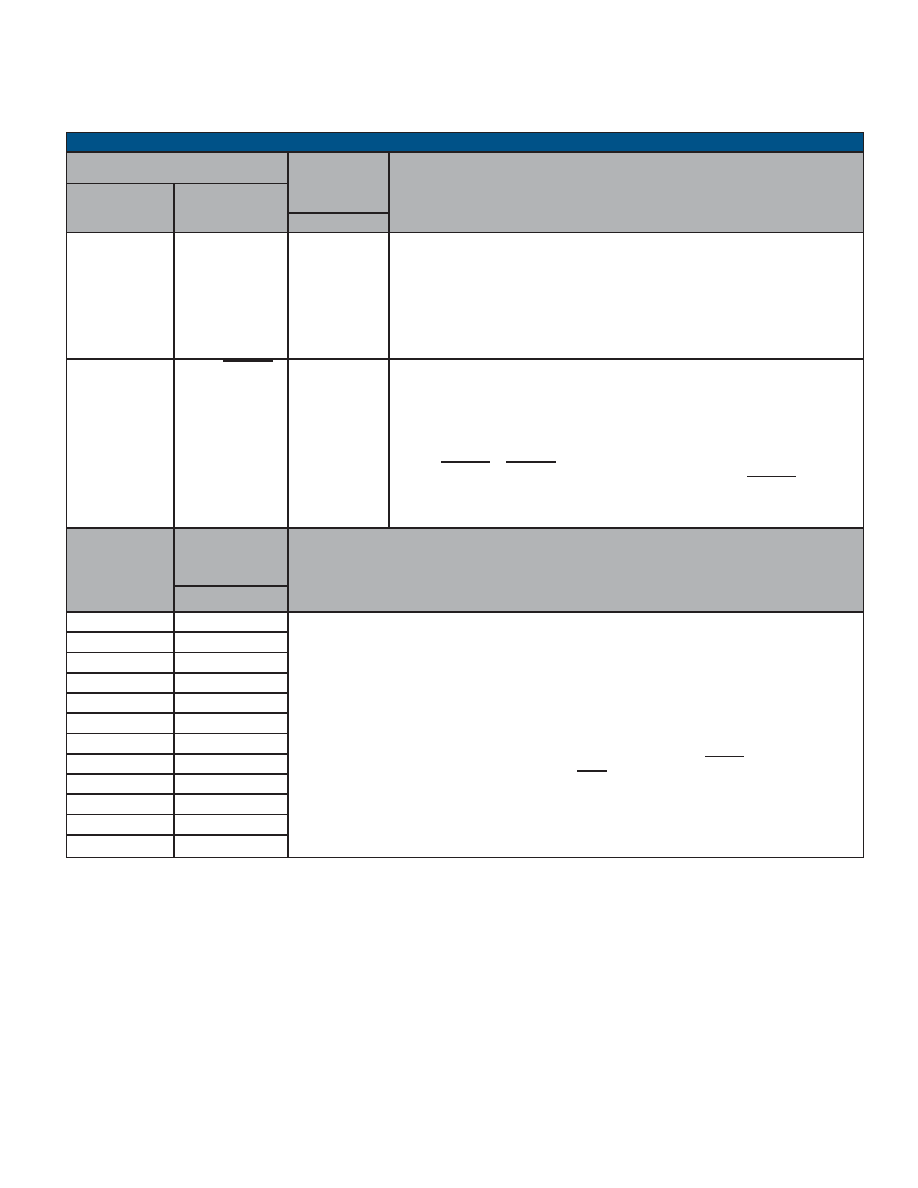
1
Lower 12 bits of 16-bit bi-directional address bus.
In both the buffered and transparent modes, the host CPU accesses Mark3 registers and internal RAM by
means of A11 - A0 (4K versions). For 64K versions, A15-A12 are also used for this purpose.
In buffered mode, A12-A0 (or A15-A0) are inputs only. In the transparent mode, A12-A0 (or A15-A0) are
inputs during CPU accesses and become outputs, driving outward (towards the CPU) when the 1553 pro-
tocol/memory management logic accesses up to 64K words of external RAM.
In transparent mode, the address bus is driven outward only when the signal DTACK is low (indicating that
the Mark3 has control of the RAM interface bus) and IOEN is high, indicating a non-host access. Most of
the time, including immediately after power turn-on, A12-A0 (or A15-A0) will be in high impedance (input)
state.
A10
2
A09
75
A08
7
A07
12
A06
27
A05
74
A04
78
A03
13
A02
19
A01
33
A00 (LSB)
18
SIGNAL NAME
DESCRIPTION
BU-6474XF/GX
BU-6484XF/GX
BU-64863F/GX
PIN
A13 /
+3.3V/+5.0V
LOGIC
77
For 64K RAM versions, this signal is always configured as address line A13. Refer to
the description for A11-A0 below.
For 4K RAM versions, if UPADDREN is connected to logic "1", this signal operates as A13.
For 4K RAM versions, if UPADDREN is connected to logic "0", then this signal MUST
be connected to +3.3V-LOGIC (logic "1") for the BU-64XX3 or +5.0V (logic "1") for the
BU-64XX5.
A13
A12 / RTBOOT
76
For 64K RAM versions, this signal is always configured as address line A12. Refer to
the description for A11-A0 below.
For 4K RAM versions, if UPADDREN is connected to logic "1", this signal operates as
A12.
For 4K RAM versions, if UPADDREN is connected to logic "0", then this signal func-
tions as RTBOOT. If RTBOOT is connected to logic "0", the Mark3 will initialize in RT
mode with the Busy status word bit set following power turn-on. If RTBOOT is hard-
wired to logic "1", the Mark3 will initialize in either Idle mode (for an RT-only part), or in
BC mode (for a BC/RT/MT part).
A12
TABLE 52. PROCESSOR ADDRESS BUS (CONT.)
SIGNAL NAME
DESCRIPTION
BU-6474XF/GX
BU-6484XF/GX
BU-64863F/GX
PIN
4K RAM
(BU-6474XF/GX
BU-6484XF/GX)
64K RAM
(BU-64863F/GX)
FLAT PACK AND GULL WING PACKAGES - SIGNAL DESCRIPTIONS BY FUNCTIONAL GROUPS (CONT.)
相关PDF资料 |
PDF描述 |
|---|---|
| A42MX24-3VQ100B | 40MX and 42MX FPGA Families |
| A42MX36-2PQ100B | 40MX and 42MX FPGA Families |
| A42MX36-2PQ100ES | 40MX and 42MX FPGA Families |
| A42MX36-2TQ100 | 40MX and 42MX FPGA Families |
| A42MX36-2TQ100A | 40MX and 42MX FPGA Families |
相关代理商/技术参数 |
参数描述 |
|---|---|
| A42MX24-FPL84 | 功能描述:IC FPGA MX SGL CHIP 36K 84-PLCC RoHS:否 类别:集成电路 (IC) >> 嵌入式 - FPGA(现场可编程门阵列) 系列:MX 标准包装:40 系列:SX-A LAB/CLB数:6036 逻辑元件/单元数:- RAM 位总计:- 输入/输出数:360 门数:108000 电源电压:2.25 V ~ 5.25 V 安装类型:表面贴装 工作温度:0°C ~ 70°C 封装/外壳:484-BGA 供应商设备封装:484-FPBGA(27X27) |
| A42MX24-FPLG84 | 功能描述:IC FPGA MX SGL CHIP 36K 84-PLCC RoHS:是 类别:集成电路 (IC) >> 嵌入式 - FPGA(现场可编程门阵列) 系列:MX 标准包装:40 系列:SX-A LAB/CLB数:6036 逻辑元件/单元数:- RAM 位总计:- 输入/输出数:360 门数:108000 电源电压:2.25 V ~ 5.25 V 安装类型:表面贴装 工作温度:0°C ~ 70°C 封装/外壳:484-BGA 供应商设备封装:484-FPBGA(27X27) |
| A42MX24-FPQ160 | 功能描述:IC FPGA MX SGL CHIP 36K 160-PQFP RoHS:否 类别:集成电路 (IC) >> 嵌入式 - FPGA(现场可编程门阵列) 系列:MX 标准包装:40 系列:SX-A LAB/CLB数:6036 逻辑元件/单元数:- RAM 位总计:- 输入/输出数:360 门数:108000 电源电压:2.25 V ~ 5.25 V 安装类型:表面贴装 工作温度:0°C ~ 70°C 封装/外壳:484-BGA 供应商设备封装:484-FPBGA(27X27) |
| A42MX24-FPQ208 | 功能描述:IC FPGA MX SGL CHIP 36K 160-PQFP RoHS:否 类别:集成电路 (IC) >> 嵌入式 - FPGA(现场可编程门阵列) 系列:MX 标准包装:40 系列:SX-A LAB/CLB数:6036 逻辑元件/单元数:- RAM 位总计:- 输入/输出数:360 门数:108000 电源电压:2.25 V ~ 5.25 V 安装类型:表面贴装 工作温度:0°C ~ 70°C 封装/外壳:484-BGA 供应商设备封装:484-FPBGA(27X27) |
| A42MX24-FPQG160 | 功能描述:IC FPGA MX SGL CHIP 36K 160-PQFP RoHS:是 类别:集成电路 (IC) >> 嵌入式 - FPGA(现场可编程门阵列) 系列:MX 标准包装:40 系列:SX-A LAB/CLB数:6036 逻辑元件/单元数:- RAM 位总计:- 输入/输出数:360 门数:108000 电源电压:2.25 V ~ 5.25 V 安装类型:表面贴装 工作温度:0°C ~ 70°C 封装/外壳:484-BGA 供应商设备封装:484-FPBGA(27X27) |
发布紧急采购,3分钟左右您将得到回复。