- 您现在的位置:买卖IC网 > PDF目录298744 > A42MX24-3VQ100A (Electronic Theatre Controls, Inc.) 40MX and 42MX FPGA Families PDF资料下载
参数资料
| 型号: | A42MX24-3VQ100A |
| 厂商: | Electronic Theatre Controls, Inc. |
| 英文描述: | 40MX and 42MX FPGA Families |
| 中文描述: | 40MX和42MX FPGA系列 |
| 文件页数: | 50/93页 |
| 文件大小: | 854K |
| 代理商: | A42MX24-3VQ100A |
第1页第2页第3页第4页第5页第6页第7页第8页第9页第10页第11页第12页第13页第14页第15页第16页第17页第18页第19页第20页第21页第22页第23页第24页第25页第26页第27页第28页第29页第30页第31页第32页第33页第34页第35页第36页第37页第38页第39页第40页第41页第42页第43页第44页第45页第46页第47页第48页第49页当前第50页第51页第52页第53页第54页第55页第56页第57页第58页第59页第60页第61页第62页第63页第64页第65页第66页第67页第68页第69页第70页第71页第72页第73页第74页第75页第76页第77页第78页第79页第80页第81页第82页第83页第84页第85页第86页第87页第88页第89页第90页第91页第92页第93页
54
Data Device Corporation
www.ddc-web.com
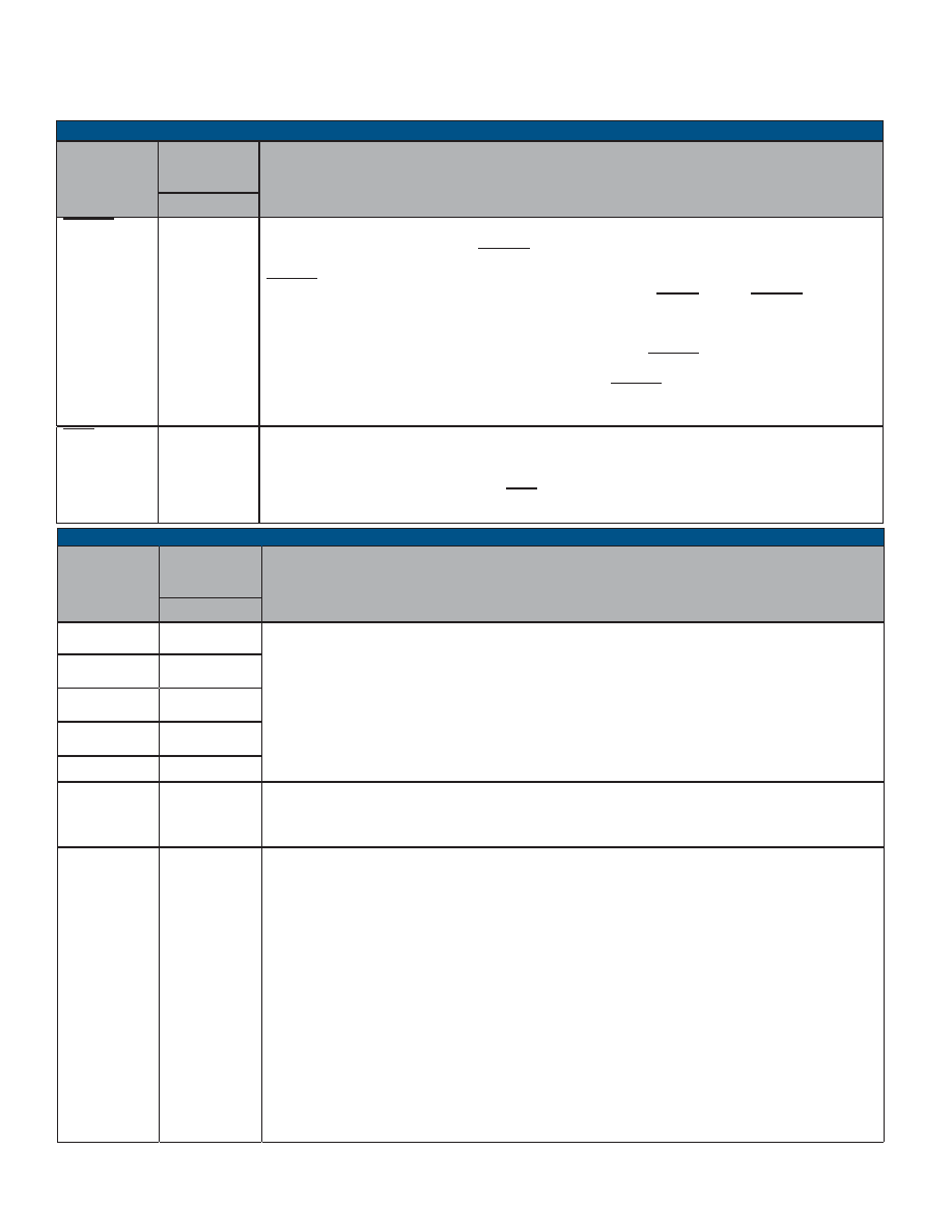
BU-6474X/6484X/6486X
J-07/05-0
IOEN(O)
64
I/O Enable.
Tri-state control for external address and data buffers. Generally not used in buffered mode. When low, indi-
cates that the Mark3 is currently performing a host access to an internal register, or internal (for transparent
mode) external RAM. In transparent mode, IOEN (low) should be used to enable external address and data
bus tri-state buffers.
READYD (O)
62
Handshake output to host processor.
For a nonzero wait state read access, READYD is asserted at the end of a host transfer cycle to indicate that
data is available to be read on D15 through D0 when asserted (low). For a nonzero wait state write cycle,
READYD is asserted at the end of the cycle to indicate that data has been transferred to a register or RAM
location. For both nonzero wait reads and writes, the host must assert STRBD low until READYD is asserted
low.
In the (buffered) zero wait state mode, this output is normally logic "1", indicating that the Mark3 is in a state
ready to accept a subsequent host transfer cycle. In zero wait mode, READYD will transition from high to low
during (or just after) a host transfer cycle, when the Mark3 initiates its internal transfer to or from registers or
internal RAM. When the Mark3 completes its internal transfer, READYD returns to logic "1", indicating it is
ready for the host to initiate a subsequent transfer cycle.
TABLE 53. PROCESSOR INTERFACE CONTROL (CONT.)
SIGNAL NAME
DESCRIPTION
BU-6474XF/GX
BU-6484XF/GX
BU-64863F/GX
PIN
RTAD4 (MSB) (I)
40
RT Address input.
If bit 5 of Configuration Register #6, RT ADDRESS SOURCE, is programmed to logic "0" (default), then the
Mark3's RT address is provided by means of these 5 input signals. In addition, if RT ADDRESS SOURCE is
logic "0", the source of RT address parity is RTADP.
There are many methods for using these input signals for designating the Mark3's RT address. For details,
refer to the description of RT_AD_LAT.
If RT ADDRESS SOURCE is programmed to logic "1", then the Mark3's source for its RT address and parity is
under software control, via data lines D5-D0. In this case, the RTAD4-RTAD0 and RTADP signals are not used.
RTAD3 (I)
39
RTAD2 (I)
24
RTAD1 (I)
45
RTAD0 (LSB) (I)
38
RT_AD_LAT (I)
36
RT Address Latch.
Input signal used to control the Mark3's internal RT address latch. If RT_AD_LAT is connected to logic "0", then
the Mark3 RT is configured to accept a hardwired (transparent) RT address from RTAD4-RTAD0 and RTADP.
If RT_AD_LAT is initially logic "0", and then transitions to logic "1", the values presented on RTAD4-RTAD0
and RTADP will be latched internally on the rising edge of RT_AD_LAT.
If RT_AD_LAT is connected to logic "1", then the Mark3's RT address is latchable under host processor con-
trol. In this case, there are two possibilities: (1) If bit 5 of Configuration Register #6, RT ADDRESS SOURCE,
is programmed to logic "0" (default), then the source of the RT Address is the RTAD4-RTAD0 and RTADP
input signals. (2) If RT ADDRESS SOURCE is programmed to logic "1", then the source of the RT Address is
the lower 6 bits of the processor data bus, D5-D1 (for RTAD4-0) and D0 (for RTADP).
In either of these two cases (with RT_AD_LAT = "1"), the processor will cause the RT address to be latched
by: (1) Writing bit 15 of Configuration Register #3, ENHANCED MODE ENABLE, to logic "1". (2) Writing bit 3
of Configuration Register #4, LATCH RT ADDRESS WITH CONFIGURATION REGISTER #5, to logic "1". (3)
Writing to Configuration Register #5. In the case of RT ADDRESS SOURCE = "1", then the values of RT
address and RT address parity must be written to the lower 6 bits of Configuration Register #5, via D5-D0. In
the case where RT ADDRESS SOURCE = "0", the bit values presented on D5-D0 become "don't care".
RTADP (I)
44
Remote Terminal Address Parity.
This input signal must provide an odd parity sum with RTAD4-RTAD0 in order for the RT to respond to non-broad-
cast commands. That is, there must be an odd number of logic "1"s from among RTAD-4-RTAD0 and RTADP.
TABLE 54. RT ADDRESS
SIGNAL NAME
DESCRIPTION
BU-6474XF/GX
BU-6484XF/GX
BU-64863F/GX
PIN
FLAT PACK AND GULL WING PACKAGES - SIGNAL DESCRIPTIONS BY FUNCTIONAL GROUPS (CONT.)
相关PDF资料 |
PDF描述 |
|---|---|
| A42MX24-3VQ100B | 40MX and 42MX FPGA Families |
| A42MX36-2PQ100B | 40MX and 42MX FPGA Families |
| A42MX36-2PQ100ES | 40MX and 42MX FPGA Families |
| A42MX36-2TQ100 | 40MX and 42MX FPGA Families |
| A42MX36-2TQ100A | 40MX and 42MX FPGA Families |
相关代理商/技术参数 |
参数描述 |
|---|---|
| A42MX24-FPL84 | 功能描述:IC FPGA MX SGL CHIP 36K 84-PLCC RoHS:否 类别:集成电路 (IC) >> 嵌入式 - FPGA(现场可编程门阵列) 系列:MX 标准包装:40 系列:SX-A LAB/CLB数:6036 逻辑元件/单元数:- RAM 位总计:- 输入/输出数:360 门数:108000 电源电压:2.25 V ~ 5.25 V 安装类型:表面贴装 工作温度:0°C ~ 70°C 封装/外壳:484-BGA 供应商设备封装:484-FPBGA(27X27) |
| A42MX24-FPLG84 | 功能描述:IC FPGA MX SGL CHIP 36K 84-PLCC RoHS:是 类别:集成电路 (IC) >> 嵌入式 - FPGA(现场可编程门阵列) 系列:MX 标准包装:40 系列:SX-A LAB/CLB数:6036 逻辑元件/单元数:- RAM 位总计:- 输入/输出数:360 门数:108000 电源电压:2.25 V ~ 5.25 V 安装类型:表面贴装 工作温度:0°C ~ 70°C 封装/外壳:484-BGA 供应商设备封装:484-FPBGA(27X27) |
| A42MX24-FPQ160 | 功能描述:IC FPGA MX SGL CHIP 36K 160-PQFP RoHS:否 类别:集成电路 (IC) >> 嵌入式 - FPGA(现场可编程门阵列) 系列:MX 标准包装:40 系列:SX-A LAB/CLB数:6036 逻辑元件/单元数:- RAM 位总计:- 输入/输出数:360 门数:108000 电源电压:2.25 V ~ 5.25 V 安装类型:表面贴装 工作温度:0°C ~ 70°C 封装/外壳:484-BGA 供应商设备封装:484-FPBGA(27X27) |
| A42MX24-FPQ208 | 功能描述:IC FPGA MX SGL CHIP 36K 160-PQFP RoHS:否 类别:集成电路 (IC) >> 嵌入式 - FPGA(现场可编程门阵列) 系列:MX 标准包装:40 系列:SX-A LAB/CLB数:6036 逻辑元件/单元数:- RAM 位总计:- 输入/输出数:360 门数:108000 电源电压:2.25 V ~ 5.25 V 安装类型:表面贴装 工作温度:0°C ~ 70°C 封装/外壳:484-BGA 供应商设备封装:484-FPBGA(27X27) |
| A42MX24-FPQG160 | 功能描述:IC FPGA MX SGL CHIP 36K 160-PQFP RoHS:是 类别:集成电路 (IC) >> 嵌入式 - FPGA(现场可编程门阵列) 系列:MX 标准包装:40 系列:SX-A LAB/CLB数:6036 逻辑元件/单元数:- RAM 位总计:- 输入/输出数:360 门数:108000 电源电压:2.25 V ~ 5.25 V 安装类型:表面贴装 工作温度:0°C ~ 70°C 封装/外壳:484-BGA 供应商设备封装:484-FPBGA(27X27) |
发布紧急采购,3分钟左右您将得到回复。