- 您现在的位置:买卖IC网 > PDF目录298744 > A42MX24-3VQ100A (Electronic Theatre Controls, Inc.) 40MX and 42MX FPGA Families PDF资料下载
参数资料
| 型号: | A42MX24-3VQ100A |
| 厂商: | Electronic Theatre Controls, Inc. |
| 英文描述: | 40MX and 42MX FPGA Families |
| 中文描述: | 40MX和42MX FPGA系列 |
| 文件页数: | 67/93页 |
| 文件大小: | 854K |
| 代理商: | A42MX24-3VQ100A |
第1页第2页第3页第4页第5页第6页第7页第8页第9页第10页第11页第12页第13页第14页第15页第16页第17页第18页第19页第20页第21页第22页第23页第24页第25页第26页第27页第28页第29页第30页第31页第32页第33页第34页第35页第36页第37页第38页第39页第40页第41页第42页第43页第44页第45页第46页第47页第48页第49页第50页第51页第52页第53页第54页第55页第56页第57页第58页第59页第60页第61页第62页第63页第64页第65页第66页当前第67页第68页第69页第70页第71页第72页第73页第74页第75页第76页第77页第78页第79页第80页第81页第82页第83页第84页第85页第86页第87页第88页第89页第90页第91页第92页第93页
40MX and 42MX FPGA Families
v6.0
1-1
40MX and 42MX FPGA Families
General Description
Actel's 40MX and 42MX families offer a cost-effective
design solution at 5V. The MX devices are single-chip
solutions
and
provide
high
performance
while
shortening the system design and development cycle.
MX
devices
can
integrate
and
consolidate
logic
implemented in multiple PALs, CPLDs, and FPGAs.
Example applications include high-speed controllers and
address decoding, peripheral bus interfaces, DSP, and co-
processor functions.
The MX device architecture is based on Actel’s patented
antifuse technology implemented in a 0.45m triple-
metal CMOS process. With capacities ranging from 3,000
to 54,000 system gates, the MX devices provide
performance up to 250 MHz, are live on power-up and
have one-fifth the standby power consumption of
comparable FPGAs. Actel’s MX FPGAs provide up to 202
user I/Os and are available in a wide variety of packages
and speed grades.
Actel’s A42MX24 and A42MX36 devices also feature
MultiPlex I/Os, which support mixed-voltage systems,
enable programmable PCI, deliver high-performance
operation at both 5.0V and 3.3V, and provide a low-
power mode. The devices are fully compliant with the
PCI Local Bus Specification (version 2.1). They deliver
200 MHz on-chip operation and 6.1 ns clock-to-output
performance.
The 42MX24 and 42MX36 devices include system-level
features such as IEEE Standard 1149.1 (JTAG) Boundary
Scan Testing and fast wide-decode modules. In addition,
the
A42MX36
device
offers
dual-port
SRAM
for
implementing fast FIFOs, LIFOs, and temporary data
storage. The storage elements can efficiently address
applications requiring wide datapath manipulation and
can perform transformation functions such as those
required for telecommunications, networking, and DSP.
All MX devices are fully tested over automotive and
military temperature ranges. In addition, the largest
member of the family, the A42MX36, is available in both
CQ208 and CQ256 ceramic packages screened to MIL-
STD-883 levels. For easy prototyping and conversion from
plastic to ceramic, the CQ208 and PQ208 devices are pin-
compatible.
MX Architectural Overview
The MX devices are composed of fine-grained building
blocks that enable fast, efficient logic designs. All devices
within these families are composed of logic modules, I/O
modules, routing resources and clock networks, which
are the building blocks for fast logic designs. In addition,
the A42MX36 device contains embedded dual-port
SRAM modules, which are optimized for high-speed
datapath functions such as FIFOs, LIFOs and scratchpad
memory. A42MX24 and A42MX36 also contain wide-
decode modules.
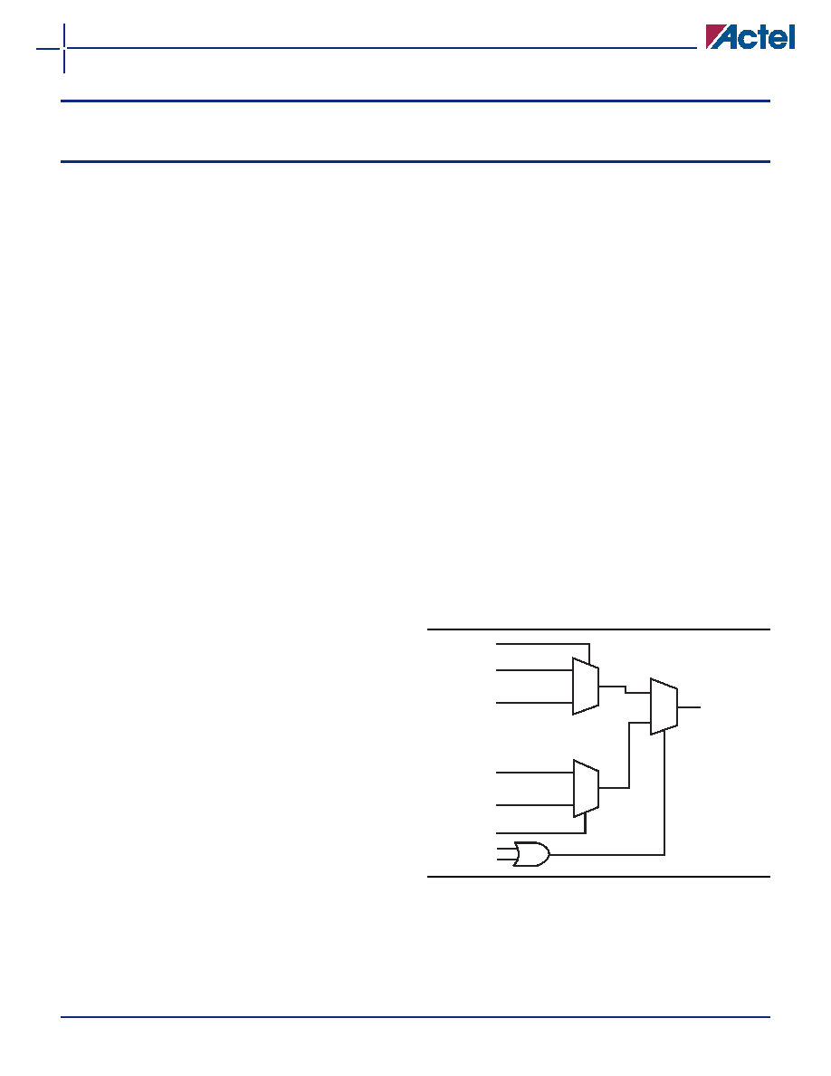
Logic Modules
The 40MX logic module is an eight-input, one-output
logic circuit designed to implement a wide range of logic
functions with efficient use of interconnect routing
resources (Figure 1-1).
The logic module can implement the four basic logic
functions (NAND, AND, OR and NOR) in gates of two,
three, or four inputs. The logic module can also
implement a variety of D-latches, exclusivity functions,
AND-ORs and OR-ANDs. No dedicated hard-wired latches
or flip-flops are required in the array; latches and flip-
flops can be constructed from logic modules whenever
required in the application.
Figure 1-1 40MX Logic Module
相关PDF资料 |
PDF描述 |
|---|---|
| A42MX24-3VQ100B | 40MX and 42MX FPGA Families |
| A42MX36-2PQ100B | 40MX and 42MX FPGA Families |
| A42MX36-2PQ100ES | 40MX and 42MX FPGA Families |
| A42MX36-2TQ100 | 40MX and 42MX FPGA Families |
| A42MX36-2TQ100A | 40MX and 42MX FPGA Families |
相关代理商/技术参数 |
参数描述 |
|---|---|
| A42MX24-FPL84 | 功能描述:IC FPGA MX SGL CHIP 36K 84-PLCC RoHS:否 类别:集成电路 (IC) >> 嵌入式 - FPGA(现场可编程门阵列) 系列:MX 标准包装:40 系列:SX-A LAB/CLB数:6036 逻辑元件/单元数:- RAM 位总计:- 输入/输出数:360 门数:108000 电源电压:2.25 V ~ 5.25 V 安装类型:表面贴装 工作温度:0°C ~ 70°C 封装/外壳:484-BGA 供应商设备封装:484-FPBGA(27X27) |
| A42MX24-FPLG84 | 功能描述:IC FPGA MX SGL CHIP 36K 84-PLCC RoHS:是 类别:集成电路 (IC) >> 嵌入式 - FPGA(现场可编程门阵列) 系列:MX 标准包装:40 系列:SX-A LAB/CLB数:6036 逻辑元件/单元数:- RAM 位总计:- 输入/输出数:360 门数:108000 电源电压:2.25 V ~ 5.25 V 安装类型:表面贴装 工作温度:0°C ~ 70°C 封装/外壳:484-BGA 供应商设备封装:484-FPBGA(27X27) |
| A42MX24-FPQ160 | 功能描述:IC FPGA MX SGL CHIP 36K 160-PQFP RoHS:否 类别:集成电路 (IC) >> 嵌入式 - FPGA(现场可编程门阵列) 系列:MX 标准包装:40 系列:SX-A LAB/CLB数:6036 逻辑元件/单元数:- RAM 位总计:- 输入/输出数:360 门数:108000 电源电压:2.25 V ~ 5.25 V 安装类型:表面贴装 工作温度:0°C ~ 70°C 封装/外壳:484-BGA 供应商设备封装:484-FPBGA(27X27) |
| A42MX24-FPQ208 | 功能描述:IC FPGA MX SGL CHIP 36K 160-PQFP RoHS:否 类别:集成电路 (IC) >> 嵌入式 - FPGA(现场可编程门阵列) 系列:MX 标准包装:40 系列:SX-A LAB/CLB数:6036 逻辑元件/单元数:- RAM 位总计:- 输入/输出数:360 门数:108000 电源电压:2.25 V ~ 5.25 V 安装类型:表面贴装 工作温度:0°C ~ 70°C 封装/外壳:484-BGA 供应商设备封装:484-FPBGA(27X27) |
| A42MX24-FPQG160 | 功能描述:IC FPGA MX SGL CHIP 36K 160-PQFP RoHS:是 类别:集成电路 (IC) >> 嵌入式 - FPGA(现场可编程门阵列) 系列:MX 标准包装:40 系列:SX-A LAB/CLB数:6036 逻辑元件/单元数:- RAM 位总计:- 输入/输出数:360 门数:108000 电源电压:2.25 V ~ 5.25 V 安装类型:表面贴装 工作温度:0°C ~ 70°C 封装/外壳:484-BGA 供应商设备封装:484-FPBGA(27X27) |
发布紧急采购,3分钟左右您将得到回复。