- 您现在的位置:买卖IC网 > PDF目录373890 > AD6634BBC (ANALOG DEVICES INC) 80 MSPS, Dual-Channel WCDMA Receive Signal Processor (RSP) PDF资料下载
参数资料
| 型号: | AD6634BBC |
| 厂商: | ANALOG DEVICES INC |
| 元件分类: | 无绳电话/电话 |
| 英文描述: | 80 MSPS, Dual-Channel WCDMA Receive Signal Processor (RSP) |
| 中文描述: | TELECOM, CELLULAR, BASEBAND CIRCUIT, PBGA196 |
| 封装: | 15 MM X 15 MM, BGA-196 |
| 文件页数: | 21/52页 |
| 文件大小: | 925K |
| 代理商: | AD6634BBC |
第1页第2页第3页第4页第5页第6页第7页第8页第9页第10页第11页第12页第13页第14页第15页第16页第17页第18页第19页第20页当前第21页第22页第23页第24页第25页第26页第27页第28页第29页第30页第31页第32页第33页第34页第35页第36页第37页第38页第39页第40页第41页第42页第43页第44页第45页第46页第47页第48页第49页第50页第51页第52页
REV. 0
AD6634
–21–
Gain Switching
The AD6634 includes circuitry that is useful in applications where
either large dynamic ranges exist or where gain ranging convert-
ers are employed. This circuitry allows digital thresholds to be
set such that an upper and a lower threshold can be programmed.
One such use of this may be to detect when an ADC is about to
reach full scale with a particular input condition. The results
would be to provide a flag that could be used to quickly insert
an attenuator that would prevent ADC overdrive. If 18 dB (or
any arbitrary value) of attenuation (or gain) is switched in, the
signal dynamic range of the system will have been increased by
18 dB. The process begins when the input signal reaches the
upper programmed threshold. In a typical application, this may
be set 1 dB (user-definable) below full scale. When this input
condition is met, the appropriate LI (LIA-A, LIA-B, LIB-A, or
LIB-B) signal associated with either the A or B input port is
made active. This can be used to switch the gain or attenuation
of the external circuit. The LI line stays active until the input
condition falls below the lower programmed threshold. In order
to provide hysteresis, a dwell time register (see Memory Map for
Input Control Registers) is available to hold off switching of the
control line for a predetermined number of clocks. Once the
input condition is below the lower threshold, the programmable
counter begins counting high speed clocks. As long as the input
signal stays below the lower threshold for the number of high
speed clock cycles programmed, the attenuator will be removed
on the terminal count. However, if the input condition goes
above the lower threshold with the counter running, it will be
reset and must fall below the lower threshold again to initiate the
process. This will prevent unnecessary switching between states
and is illustrated in Figure 27.
When the input signal goes above the upper threshold, the
appropriate LI signal becomes active. Once the signal falls
below the lower threshold, the counter begins counting. If the
input condition goes above the lower threshold, the counter is
reset and starts again as shown in Figure 27. Once the counter
has terminated to 0, the LI line goes inactive.
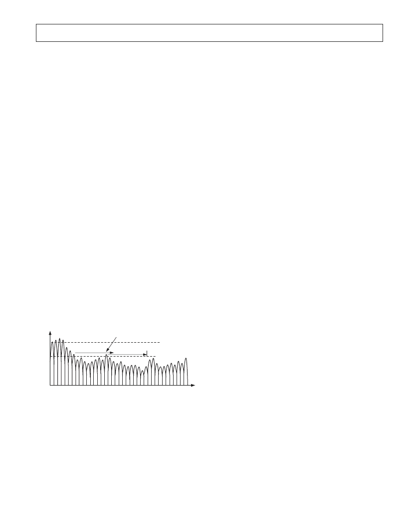
“HIGH”
M
DWELL TIME
“LOW”
UPPER
THRESHOLD
LOWER
THRESHOLD
COUNTER
RESTARTS
TIME
Figure 27. Threshold Settings for LI
The LI line can be used for a variety of functions. It can be used
to set the controls of an attenuator, DVGA, or integrated and used
with an analog VGA. To simplify the use of this feature, the
AD6634 includes two separate gain settings, one when this line is
inactive (rCIC2_QUIET[4:0] stored in bits 9:5 of 0x92 register)
and the other when active (rCIC2_LOUD[4:0] stored in bits
4:0 of 0x92 register). This allows the digital gain to be adjusted
to the external changes. In conjunction with the gain setting, a
variable hold-off is included to compensate for the pipeline delay
of the ADC and the switching time of the gain control element.
Together, these two features provide seamless gain switching.
Another use of this pin is to facilitate a gain range hold-off within a
gain ranging ADC. For converters that use gain ranging to increase
total signal dynamic range, it may be desirable to prohibit internal
gain ranging from occurring in some instances. For such converters,
the LI (A or B) line can be used to hold this off. For this applica-
tion, the upper threshold would be set based on similar criteria.
However, the lower threshold would be set to a level consistent
with the gain ranges of the specific converter. The hold-off delay
can then be set appropriately for any of a number of factors such
as fading profile, signal peak to average ratio, or any other time-
based characteristics that might cause unnecessary gain changes.
Since the AD6634 has a total of four gain control circuits that
can be used if both A and B input ports have interleaved data.
Each respective LI pin is independent and can be set to differ-
ent set points. It should be noted that the gain control circuits
are wideband and are implemented prior to any filtering elements
to minimize loop delay. Any of the four channels can be set to
monitor any of the possible four input channels (two in normal
mode and four when the inputs are time multiplexed).
The chip also provides appropriate scaling of the internal data
based on the attenuation associated with the LI signal. In this
manner, data to the DSP maintains a correct scale value through-
out the process, making it totally independent. Since there are
often finite delays associated with external gain switching com-
ponents, the AD6634 includes a variable pipeline delay that can
be used to compensate for external pipeline delays or gross
settling times associated with gain/attenuator devices. This delay
may be set up to seven high speed clocks. These features ensure
smooth switching between gain settings.
Input Data Scaling
The AD6634 has two data input ports, an A input port and a
B input port. Each accepts 14-bit mantissa (two’s complement
integer) IN[13:0], a 3-bit exponent (unsigned integer) EXP[2:0]
and the Input Enable(IEN). Both inputs are clocked by CLK.
These pins allow direct interfacing to both standard fixed-point
ADCs such as the AD9238 and AD6645, as well as to gain-
ranging ADCs such as the AD6600. For normal operation with
ADCs having fewer than 14 bits, the active bits should be MSB
justified and the unused LSBs should be tied low.
The 3-bit exponent, EXP[2:0] is interpreted as an unsigned
integer. The exponent will subsequently be modified by either of
rCIC2_LOUD[4:0] or rCIC2_QUIET[4:0] depending on whether
LI line is active or not. These 5-bit scale values are stored in the
rCIC2 scale register (0x92) and the scaling is applied before the
data enters the rCIC2 resampling filter. These 5-bit registers
contain scale values to compensate for the rCIC2 gain, external
attenuator (if used) and the exponent offset (Expoff). If no external
attenuator is used, both the rCIC2_QUIET and rCIC2_LOUD
registers would contain the same value. A detailed explanation
and equation for setting the attenuating scale register is given in
the Scaling with Floating-Point or Gain-Ranging ADCs section.
Scaling with Fixed-Point ADCs
For fixed-point ADCs, the AD6634 exponent inputs EXP[2:0] are
typically not used and should be tied low. The ADC outputs are
tied directly to the AD6634 Inputs, MSB-justified. The ExpOff
bits in 0x92 should be programmed to 0. Likewise, the Exponent
Invert bit should be 0. Thus for fixed-point ADCs, the exponents
are typically static and no input scaling is used in the AD6634.
相关PDF资料 |
PDF描述 |
|---|---|
| AD6634PCB | 80 MSPS, Dual-Channel WCDMA Receive Signal Processor (RSP) |
| AD6635 | 4-Channel, 80 MSPS WCDMA Receive Signal Processor (RSP) |
| AD6635BB | 4-Channel, 80 MSPS WCDMA Receive Signal Processor (RSP) |
| AD6636 | 150 MSPS Wideband Digital Down-Converter (DDC) |
| AD6636BBCZ1 | 150 MSPS Wideband Digital Down-Converter (DDC) |
相关代理商/技术参数 |
参数描述 |
|---|---|
| AD6634BBCZ | 功能描述:IC RSP 80MSPS DUAL 196CSPBGA RoHS:是 类别:RF/IF 和 RFID >> RF 混频器 系列:AD6634 产品培训模块:Lead (SnPb) Finish for COTS Obsolescence Mitigation Program 标准包装:100 系列:- RF 型:W-CDMA 频率:2.11GHz ~ 2.17GHz 混频器数目:1 增益:17dB 噪音数据:2.2dB 次要属性:- 电流 - 电源:11.7mA 电源电压:2.7 V ~ 3.3 V 包装:托盘 封装/外壳:12-VFQFN 裸露焊盘 供应商设备封装:12-QFN-EP(3x3) |
| AD6634BC/PCB | 制造商:Analog Devices 功能描述:WCDMA RECEIVE SGNL PROCESSOR - Bulk |
| AD6634PCB | 制造商:AD 制造商全称:Analog Devices 功能描述:80 MSPS, Dual-Channel WCDMA Receive Signal Processor (RSP) |
| AD6635 | 制造商:AD 制造商全称:Analog Devices 功能描述:4-Channel, 80 MSPS WCDMA Receive Signal Processor (RSP) |
| AD6635BB | 功能描述:IC RSP 80MSPS QUAD 324-BGA RoHS:否 类别:RF/IF 和 RFID >> RF 混频器 系列:AD6635 产品培训模块:Lead (SnPb) Finish for COTS Obsolescence Mitigation Program 标准包装:100 系列:- RF 型:W-CDMA 频率:2.11GHz ~ 2.17GHz 混频器数目:1 增益:17dB 噪音数据:2.2dB 次要属性:- 电流 - 电源:11.7mA 电源电压:2.7 V ~ 3.3 V 包装:托盘 封装/外壳:12-VFQFN 裸露焊盘 供应商设备封装:12-QFN-EP(3x3) |
发布紧急采购,3分钟左右您将得到回复。