- 您现在的位置:买卖IC网 > PDF目录373890 > AD6634BBC (ANALOG DEVICES INC) 80 MSPS, Dual-Channel WCDMA Receive Signal Processor (RSP) PDF资料下载
参数资料
| 型号: | AD6634BBC |
| 厂商: | ANALOG DEVICES INC |
| 元件分类: | 无绳电话/电话 |
| 英文描述: | 80 MSPS, Dual-Channel WCDMA Receive Signal Processor (RSP) |
| 中文描述: | TELECOM, CELLULAR, BASEBAND CIRCUIT, PBGA196 |
| 封装: | 15 MM X 15 MM, BGA-196 |
| 文件页数: | 36/52页 |
| 文件大小: | 925K |
| 代理商: | AD6634BBC |
第1页第2页第3页第4页第5页第6页第7页第8页第9页第10页第11页第12页第13页第14页第15页第16页第17页第18页第19页第20页第21页第22页第23页第24页第25页第26页第27页第28页第29页第30页第31页第32页第33页第34页第35页当前第36页第37页第38页第39页第40页第41页第42页第43页第44页第45页第46页第47页第48页第49页第50页第51页第52页
REV. 0
–36–
AD6634
LINK PORT
A OR B
AGC A I, Q
(4 BYTES)
AGC B I, Q
(4 BYTES)
AGC A I, Q
(4 BYTES)
AGC B I, Q
(4 BYTES)
ADDR 0x1B OR 0x1D BIT 0 = 1, BIT 1 = 0, BIT 2 = 0
LINK PORT
A OR B
AGC A I, Q
(4 BYTES)
AGC A RSSI
(4 BYTES)
AGC B I, Q
(4 BYTES)
AGC B RSSI
(4 BYTES)
ADDR 0x1B OR 0x1D BIT 0 = 1, BIT 1 = 0, BIT 2 = 1
LINK PORT A
AGC A I, Q
(4 BYTES)
AGC A RSSI
(4 BYTES)
AGC A I, Q
(4 BYTES)
AGC A RSSI
(4 BYTES)
AGC B I, Q
(4 BYTES)
AGC B RSSI
(4 BYTES)
AGC B I, Q
(4 BYTES)
AGC B RSSI
(4 BYTES)
LINK PORT B
ADDR 0x1B OR 0x1D BIT 0 = 1, BIT 1 = 1, BIT 2 = 0
Figure 42. Link Port Data from AGC
Note that Bit 0 = 1 Bit 1 = 0, and Bit 2 = 1 is not a valid
configuration. Bit 2 must be set to 0 to output AGC A IQ and
RSSI words on link port A, and AGC B IQ and RSSI words
on link port B.
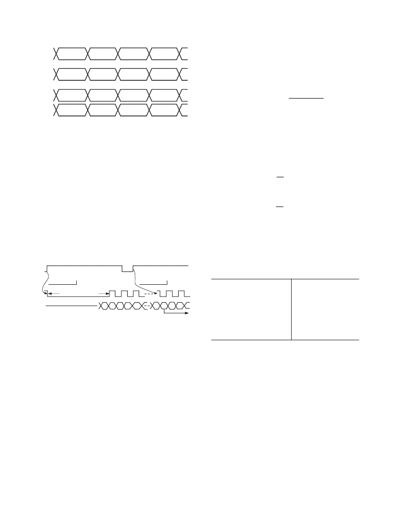
Link Port Timing
Both link ports run off of PCLK, which can be externally provided
to the chip (Addr 0x1E Bit 0 = 0) or generated from the master
clock of the AD6634 (Addr 0x1E Bit 0 = 1). This register boots
to 0 (Slave mode) and allows the user to control the data rate
coming from the AD6634. PCLK can be run as fast as 100 MHz.
The link port provides a 1-byte data-word (LA[7:0], LB[7:0]
pins) and output clocks (LACLKOUT, LBCLKOUT pins) in
response to a ready signals (LACLKIN, LBCLKIN pins) from
the receiver. Each link port transmits eight bits on each edge of
LCLKOUT, requiring eight LCLKOUT cycles to complete
transmission of the full 16 bytes of a TigerSHARC quad-word.
D0 D1 D2 D3
D4
D15
D0 D1 D2
NEXT QUAD-WORD
TigerSHARC READY TO
RECEIVE QUAD-WORD
WAIT >= 6 CYCLES
TigerSHARC READY TO
RECEIVE NEXT QUAD-WORD
LCLKIN
LCLKOUT
LDAT[7:0]
Figure 43. Link Port Data Transfer
Due to the TigerSHARC link port protocol, the AD6634 must
wait at least six PCLK cycles after the TigerSHARC is ready to
receive data, as indicated by the TigerSHARC setting the respective
AD6634 LCLKIN pin high. Once the AD6634 link port has
waited the appropriate number of PCLK cycles and has begun
transmitting data, the TigerSHARC does a connectivity check
by sending the AD6634 LCLKIN low and then high while the
data is being transmitted. This tells the AD6634 link port that the
TigerSHARC’s DMA is ready to receive the next quad-word after
completion of the current quad-word. Because the connectivity
check is done in parallel to the data transmission, the AD6634
is able to stream uninterrupted data to the TigerSHARC.
The length of the wait before data transmission is a 4-bit
programmable value in the link port control registers (0x1B and
0x1D Bits 6–3). This value allows the AD6634 PCLK and
the TigerSHARC PCLK to be run at different rates and
out of phase.
WAIT
ceil
f
f
LCLK
LCLK TSHARC
_
≥
×
6
34
_
WAIT
ensures that the amount of time the AD6634 needs to wait
to begin data transmission is at least equal to the minimum amount
of time the TigerSHARC is expecting it to wait. If the PCLK of
the AD6634 is out of phase with the PCLK of the TigerSHARC
and the argument to the ceil() function is an integer,
WAIT
must
be strictly greater than the value given in the above formula.
If the LCLKs are in phase, the maximum output data rate is:
f
f
LCLK
LCLK TSHARC
_
_
34
15
6
≤
×
otherwise it is:
f
f
LCLK
LCLK TSHARC
_
_
34
14
6
≤
×
TigerSHARC Configuration
Since the AD6634 is always the transmitter in this link and the
TigerSHARC is always the receiver, the values in Table IX can
be programmed into the LCTL register for the link port used to
receive AD6634 output data. User means that the actual register
value depends on the user’s application.
Table IX. TigerSHARC LCTLx Register Configuration
VERE
SPD
LTEN
PSIZE
TTOE
CERE
LREN
RTOE
0
User
0
1
0
0
1
1
MEMORY MAPS
0x00–0x7F: Coefficient Memory(CMEM)
This is the Coefficient Memory(C-MEM) used by the RCF
(See Table X). It is memory mapped as 128 words by 20 bits.
A second 128 words of RAM may be accessed via this same
location by writing Bit 8 of the RCF control register high at
channel address 0xA4. The filter calculated will always use the
same coefficients for I and Q. By using memory from both of these
128 blocks, a filter up to 160 taps can be calculated. Multiple
filters can be loaded and selected with a single internal access
to the Coefficient Offset register at channel address 0xA3.
相关PDF资料 |
PDF描述 |
|---|---|
| AD6634PCB | 80 MSPS, Dual-Channel WCDMA Receive Signal Processor (RSP) |
| AD6635 | 4-Channel, 80 MSPS WCDMA Receive Signal Processor (RSP) |
| AD6635BB | 4-Channel, 80 MSPS WCDMA Receive Signal Processor (RSP) |
| AD6636 | 150 MSPS Wideband Digital Down-Converter (DDC) |
| AD6636BBCZ1 | 150 MSPS Wideband Digital Down-Converter (DDC) |
相关代理商/技术参数 |
参数描述 |
|---|---|
| AD6634BBCZ | 功能描述:IC RSP 80MSPS DUAL 196CSPBGA RoHS:是 类别:RF/IF 和 RFID >> RF 混频器 系列:AD6634 产品培训模块:Lead (SnPb) Finish for COTS Obsolescence Mitigation Program 标准包装:100 系列:- RF 型:W-CDMA 频率:2.11GHz ~ 2.17GHz 混频器数目:1 增益:17dB 噪音数据:2.2dB 次要属性:- 电流 - 电源:11.7mA 电源电压:2.7 V ~ 3.3 V 包装:托盘 封装/外壳:12-VFQFN 裸露焊盘 供应商设备封装:12-QFN-EP(3x3) |
| AD6634BC/PCB | 制造商:Analog Devices 功能描述:WCDMA RECEIVE SGNL PROCESSOR - Bulk |
| AD6634PCB | 制造商:AD 制造商全称:Analog Devices 功能描述:80 MSPS, Dual-Channel WCDMA Receive Signal Processor (RSP) |
| AD6635 | 制造商:AD 制造商全称:Analog Devices 功能描述:4-Channel, 80 MSPS WCDMA Receive Signal Processor (RSP) |
| AD6635BB | 功能描述:IC RSP 80MSPS QUAD 324-BGA RoHS:否 类别:RF/IF 和 RFID >> RF 混频器 系列:AD6635 产品培训模块:Lead (SnPb) Finish for COTS Obsolescence Mitigation Program 标准包装:100 系列:- RF 型:W-CDMA 频率:2.11GHz ~ 2.17GHz 混频器数目:1 增益:17dB 噪音数据:2.2dB 次要属性:- 电流 - 电源:11.7mA 电源电压:2.7 V ~ 3.3 V 包装:托盘 封装/外壳:12-VFQFN 裸露焊盘 供应商设备封装:12-QFN-EP(3x3) |
发布紧急采购,3分钟左右您将得到回复。