- 您现在的位置:买卖IC网 > PDF目录373890 > AD6634BBC (ANALOG DEVICES INC) 80 MSPS, Dual-Channel WCDMA Receive Signal Processor (RSP) PDF资料下载
参数资料
| 型号: | AD6634BBC |
| 厂商: | ANALOG DEVICES INC |
| 元件分类: | 无绳电话/电话 |
| 英文描述: | 80 MSPS, Dual-Channel WCDMA Receive Signal Processor (RSP) |
| 中文描述: | TELECOM, CELLULAR, BASEBAND CIRCUIT, PBGA196 |
| 封装: | 15 MM X 15 MM, BGA-196 |
| 文件页数: | 50/52页 |
| 文件大小: | 925K |
| 代理商: | AD6634BBC |
第1页第2页第3页第4页第5页第6页第7页第8页第9页第10页第11页第12页第13页第14页第15页第16页第17页第18页第19页第20页第21页第22页第23页第24页第25页第26页第27页第28页第29页第30页第31页第32页第33页第34页第35页第36页第37页第38页第39页第40页第41页第42页第43页第44页第45页第46页第47页第48页第49页当前第50页第51页第52页
REV. 0
–50–
AD6634
address is set, External Address [0] DR0 must be the first data register
read to initiate an internal access. DR2 is only four bits wide.
Data written to the upper four bits of this register will be ignored.
Likewise reading from this register will produce only 4 LSBs.
Write Sequencing
Writing to an internal location is achieved by first writing the upper
two bits of the address to Bits 1 through 0 of the ACR. Bits 7:2 may
be set to select the channel as indicated above. The CAR is then
written with the lower eight bits of the internal address (it doesn’t
matter if the CAR is written before the ACR as long as both are
written before the internal access). Data Register 2 (DR2) and
Register 1 (DR1) must be written first because the write to data
register DR0 triggers the internal access. Data register DR0 must
always be the last register written to initiate the internal write.
Read Sequencing
Reading from the microport is accomplished in the same manner.
The internal address is set up the same way as the write. A read
from data register DR0 activates the internal read, thus register DR0
must always be read first to initiate an internal read followed
by DR1 and DR2. This provides the 8 LSBs of the internal read
through the microport (D[7:0]). Additional data registers can be
read to read the balance of the internal memory.
Read/Write Chaining
The microport of the AD6634 allows for multiple accesses while
CS
is held low (
CS
can be tied permanently low if the microport is
not shared with additional devices). The user can access multiple
locations by pulsing the
WR
or
RD
line and changing the contents
of the external 3-bit address bus. External access to the external
registers of Table XIII is accomplished in one of two modes
using the
CS
,
RD
,
WR
, and MODE inputs. The access modes
are Intel nonmultiplexed mode and Motorola nonmultiplexed
mode. These modes are controlled by the MODE input
(MODE = 0 for INM, MODE = 1 for MNM).
CS
,
RD
, and
WR
control the access type for each mode.
Intel Nonmultiplexed Mode (INM)
MODE must be tied Low to operate the AD6634 microprocessor
in INM mode. The access type is controlled by the user with the
CS
,
RD
(
DS
), and
WR
(RW) inputs. The RDY (
DTACK
) signal
is produced by the microport to communicate to the user that an
access has been completed. RDY (
DTACK
) goes Low at the
start of the access and is released when the internal cycle is
complete. See the timing diagrams for both the read and write
modes in the Specifications.
Motorola Nonmultiplexed Mode (MNM)
MODE must be tied High to operate the AD6634 microproces-
sor in MNM mode. The access type is controlled by the user
with the
CS
,
DS
(
RD
), and RW (
WR
) inputs. The
DTACK
(RDY) signal is produced by the microport to communicate to
the user that an access has been completed.
DTACK
(RDY) goes
Low when an internal access is complete and then will return High
after
DS
(
RD
) is deasserted. See the timing diagrams for both the
read and write modes in the Specifications.
SERIAL PORT CONTROL
The AD6634 has a serial port serving as a control interface apart
from the microport control interface. Serial port input pin (SDI)
can access all of the internal registers for all of the channels and
has pre-emptive access over the microport. In this manner, a single
DSP could be used to control the AD6634 over the serial port
control interface.
The serial control port uses the serial clock (SCLK). The
serial input port is self-framing as described below and allows
more efficient use of the serial input bandwidth for programming.
The beginning of a serial input frame is signaled by a Frame bit
that appears on the SDI pin. This is the MSB of the Serial Input
frame. After the frame bit has been sampled high on the falling
edge of SCLK, a state counter will start and enable an 11-bit
serial shifter four serial clock cycles later. These four SCLK cycles
represent the Don’t Care bits of the serial frame that are ignored.
After all of the bits are shifted, the serial input port will pass
along the 8-bit data and 3-bit address to the arbitration block.
The serial word structure for the SDI input is illustrated in
Figure 47. Only 15 bits are listed so that the second bit in a
standard 16-bit serial word is considered the frame bit. This is
done for compatibility with the AD6620 serial input port. The
shifting order begins with frame and shifts the address MSB first
and then the data MSB first.
Serial Port Timing Specifications
The AD6634 serial control channel can operate only in the slave
mode. Figures 44–46 indicate the required timing for each
specification.
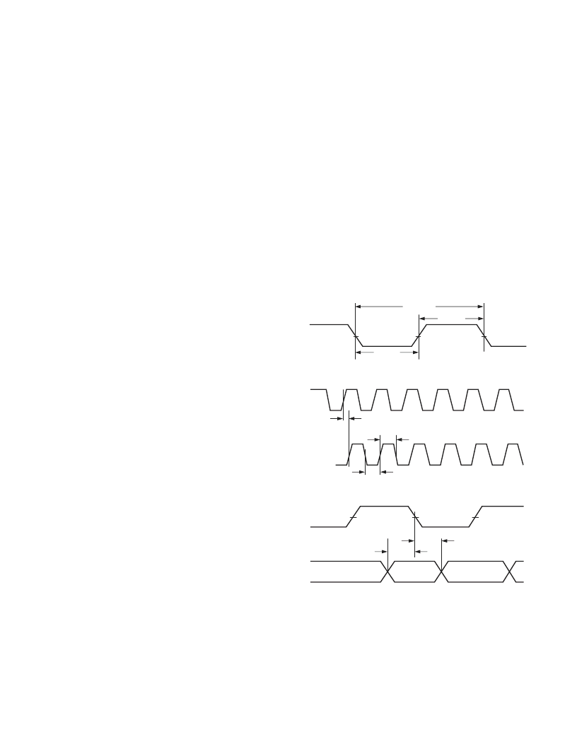
SCLK
t
SCLK
t
SCLKH
t
SCLKL
Figure 44. SCLK Timing Requirements
t
SCLKH
t
SCLKL
t
DSCLKH
CLK
SCLK
Figure 45. SCLK Switching Characteristics (Divide by 1)
t
SSI
SCLK
SDI
DATA
t
HSI
Figure 46. Serial Input Data Timing Requirements
SDI
SDI is the Serial Data Input. Serial Data is sampled on the
falling edge of SCLK. This pin is used in the serial control
mode to write the internal control registers of the AD6634.
SCLK
SCLK is a clock input and the SDI input is sampled on the
falling edge of SCLK and all outputs are switched on the rising
edge of SCLK. The maximum speed of this port is 80 MHz.
相关PDF资料 |
PDF描述 |
|---|---|
| AD6634PCB | 80 MSPS, Dual-Channel WCDMA Receive Signal Processor (RSP) |
| AD6635 | 4-Channel, 80 MSPS WCDMA Receive Signal Processor (RSP) |
| AD6635BB | 4-Channel, 80 MSPS WCDMA Receive Signal Processor (RSP) |
| AD6636 | 150 MSPS Wideband Digital Down-Converter (DDC) |
| AD6636BBCZ1 | 150 MSPS Wideband Digital Down-Converter (DDC) |
相关代理商/技术参数 |
参数描述 |
|---|---|
| AD6634BBCZ | 功能描述:IC RSP 80MSPS DUAL 196CSPBGA RoHS:是 类别:RF/IF 和 RFID >> RF 混频器 系列:AD6634 产品培训模块:Lead (SnPb) Finish for COTS Obsolescence Mitigation Program 标准包装:100 系列:- RF 型:W-CDMA 频率:2.11GHz ~ 2.17GHz 混频器数目:1 增益:17dB 噪音数据:2.2dB 次要属性:- 电流 - 电源:11.7mA 电源电压:2.7 V ~ 3.3 V 包装:托盘 封装/外壳:12-VFQFN 裸露焊盘 供应商设备封装:12-QFN-EP(3x3) |
| AD6634BC/PCB | 制造商:Analog Devices 功能描述:WCDMA RECEIVE SGNL PROCESSOR - Bulk |
| AD6634PCB | 制造商:AD 制造商全称:Analog Devices 功能描述:80 MSPS, Dual-Channel WCDMA Receive Signal Processor (RSP) |
| AD6635 | 制造商:AD 制造商全称:Analog Devices 功能描述:4-Channel, 80 MSPS WCDMA Receive Signal Processor (RSP) |
| AD6635BB | 功能描述:IC RSP 80MSPS QUAD 324-BGA RoHS:否 类别:RF/IF 和 RFID >> RF 混频器 系列:AD6635 产品培训模块:Lead (SnPb) Finish for COTS Obsolescence Mitigation Program 标准包装:100 系列:- RF 型:W-CDMA 频率:2.11GHz ~ 2.17GHz 混频器数目:1 增益:17dB 噪音数据:2.2dB 次要属性:- 电流 - 电源:11.7mA 电源电压:2.7 V ~ 3.3 V 包装:托盘 封装/外壳:12-VFQFN 裸露焊盘 供应商设备封装:12-QFN-EP(3x3) |
发布紧急采购,3分钟左右您将得到回复。