- 您现在的位置:买卖IC网 > PDF目录373890 > AD6634BBC (ANALOG DEVICES INC) 80 MSPS, Dual-Channel WCDMA Receive Signal Processor (RSP) PDF资料下载
参数资料
| 型号: | AD6634BBC |
| 厂商: | ANALOG DEVICES INC |
| 元件分类: | 无绳电话/电话 |
| 英文描述: | 80 MSPS, Dual-Channel WCDMA Receive Signal Processor (RSP) |
| 中文描述: | TELECOM, CELLULAR, BASEBAND CIRCUIT, PBGA196 |
| 封装: | 15 MM X 15 MM, BGA-196 |
| 文件页数: | 22/52页 |
| 文件大小: | 925K |
| 代理商: | AD6634BBC |
第1页第2页第3页第4页第5页第6页第7页第8页第9页第10页第11页第12页第13页第14页第15页第16页第17页第18页第19页第20页第21页当前第22页第23页第24页第25页第26页第27页第28页第29页第30页第31页第32页第33页第34页第35页第36页第37页第38页第39页第40页第41页第42页第43页第44页第45页第46页第47页第48页第49页第50页第51页第52页
REV. 0
–22–
AD6634
Table I. AD6600 Transfer Function with AD6634
ExpInv = 1, and No ExpOff
ADC Input
Level
AD6600
RSSI[2:0]
AD6634
Data
Signal
Reduction (dB)
Largest
101 (5)
100 (4)
011 (3)
010 (2)
001 (1)
000 (0)
/4 (>> 2)
/8 (>>3)
/16 (>> 4)
/32 (>> 5)
/64 (>> 6)
/128 (>> 7)
–12
–18
–24
–30
–36
–42
Smallest
(ExpInv = 1, rCIC2 Scale = 0)
Table II. AD6600 Transfer Function with AD6620
ExpInv = 1, and ExpOff = 6
ADC Input
Level
AD6600
RSSI[2:0]
AD6634
Data
Signal
Reduction (dB)
Largest
101 (5)
100 (4)
011 (3)
010 (2)
001 (1)
000 (0)
/1 (>> 0)
/2 (>> 1)
/4 (>> 2)
/8 (>> 3)
/16 (>> 4)
/32 (>> 5)
0
–6
–12
–18
–24
–30
Smallest
(ExpInv = 1, ExpOff = 30, ExpWeight = 0)
This flexibility in handling the exponent allows the AD6634 to
interface with gain-ranging ADCs other than the AD6600. The
Exponent Offset can be adjusted to allow up to seven RSSI(EXP)
ranges to be used as opposed to the AD6600’s five. It also allows
the AD6634 to be tailored in a system that employs the AD6600
but does not utilize all of its signal range. For example, if only
the first four RSSI ranges are expected to occur, the ExpOff
could be adjusted to 29, which would then make RSSI = 4
correspond to the 0 dB point of the AD6634.
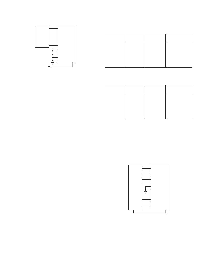
IN 13
IN 2
IN 1
IN 0
IEN
D10 (MSB)
D0 (LSB)
AD6600
AD6634
EXP 1
EXP 0
RSSI 1
RSSI 0
EXP 2
RSSI 2
AB_OUT
Figure 29. Typical Interconnection of the AD6600
Gain-Ranging ADC and the AD6634
NUMERICALLY CONTROLLED OSCILLATOR
Frequency Translation
This processing stage comprises a digital tuner consisting of two
multipliers and a 32-bit complex NCO. Each channel of the
AD6634 has an independent NCO. The NCO serves as a quadra-
ture local oscillator capable of producing an NCO frequency
between –CLK/2 and +CLK/2 with a resolution of CLK/2
32
in
the complex mode. The worst-case spurious signal from the
NCO is better than –100 dBc for all output frequencies.
IN 13
IN 2
IN 1
IN 0
EXP 2
EXP 1
EXP 0
IEN
VDD
D11 (MSB)
D0 (LSB)
AD6640
AD6634
Figure 28. Typical Interconnection of the AD6640
Fixed Point ADC and the AD6634
Scaling with Floating-Point or Gain-Ranging ADCs
An example of the exponent control feature combines the AD6600
and the AD6634. The AD6600 is an 11-bit ADC with three bits
of gain ranging. In effect, the 11-bit ADC provides the mantissa,
and the three bits of relative signal strength indicator (RSSI) for
the exponent. Only five of the eight available steps are used by
the AD6600. See the AD6600 data sheet for additional details.
For gain-ranging ADCs such as the AD6600,
SCALED INPUT
EXPINV
IN
EXPWEIGHT
MOD
EXP
rCIC
_
=
,
,
–
–
,
=
×
=
+
(
)
2
1
0
7
2 32
where,
IN
is the value of IN[13:0],
EXP
is the value of
EXP[2:0], and rCIC2 is the rCIC scale register value (0x92
Bits 9–5 and 4–0).
The RSSI output of the AD6600 numerically grows with increas-
ing signal strength of the analog input (RSSI = 5 for a large
signal, RSSI = 0 for a small signal). When the Exponent Invert
Bit (ExpInv) is set to zero, the AD6634 will consider the small-
est signal at the IN[13:0] to be the largest and as the EXP word
increases, it shifts the data down internally (EXP = 5 will shift a
14-bit word right by five internal bits before passing the data to
the rCIC2). In this example where ExpInv = 0, the AD6634
regards the largest signal possible on the AD6600 as the small-
est signal. Thus, we can use the Exponent Invert Bit to make
the AD6634 exponent agree with the AD6600 RSSI. By setting
ExpInv = 1, this forces the AD6634 to shift the data up (left)
for growing EXP instead of down. The exponent invert bit
should always be set high for use with the AD6600.
The exponent offset is used to shift the data up. For example,
Table I shows that with no rCIC2 scaling, 12 dB of range is lost
when the ADC input is at the largest level. This is undesirable
because it lowers the dynamic range and SNR of the system by reduc-
ing the signal of interest relative to the quantization noise floor.
To avoid this automatic attenuation of the full-scale ADC signal
the ExpOff is used to move the largest signal (RSSI = 5) up to
the point where there is no down shift. In other words, once the
Exponent Invert bit has been set, the exponent offset should be
adjusted so that mod(7–5 + ExpOff, 32) = 0. This is the case
when exponent offset is set to 30 since mod(32, 32) = 0.
Table II illustrates the use of ExpInv and ExpOff when used
with the AD6600 ADC.
相关PDF资料 |
PDF描述 |
|---|---|
| AD6634PCB | 80 MSPS, Dual-Channel WCDMA Receive Signal Processor (RSP) |
| AD6635 | 4-Channel, 80 MSPS WCDMA Receive Signal Processor (RSP) |
| AD6635BB | 4-Channel, 80 MSPS WCDMA Receive Signal Processor (RSP) |
| AD6636 | 150 MSPS Wideband Digital Down-Converter (DDC) |
| AD6636BBCZ1 | 150 MSPS Wideband Digital Down-Converter (DDC) |
相关代理商/技术参数 |
参数描述 |
|---|---|
| AD6634BBCZ | 功能描述:IC RSP 80MSPS DUAL 196CSPBGA RoHS:是 类别:RF/IF 和 RFID >> RF 混频器 系列:AD6634 产品培训模块:Lead (SnPb) Finish for COTS Obsolescence Mitigation Program 标准包装:100 系列:- RF 型:W-CDMA 频率:2.11GHz ~ 2.17GHz 混频器数目:1 增益:17dB 噪音数据:2.2dB 次要属性:- 电流 - 电源:11.7mA 电源电压:2.7 V ~ 3.3 V 包装:托盘 封装/外壳:12-VFQFN 裸露焊盘 供应商设备封装:12-QFN-EP(3x3) |
| AD6634BC/PCB | 制造商:Analog Devices 功能描述:WCDMA RECEIVE SGNL PROCESSOR - Bulk |
| AD6634PCB | 制造商:AD 制造商全称:Analog Devices 功能描述:80 MSPS, Dual-Channel WCDMA Receive Signal Processor (RSP) |
| AD6635 | 制造商:AD 制造商全称:Analog Devices 功能描述:4-Channel, 80 MSPS WCDMA Receive Signal Processor (RSP) |
| AD6635BB | 功能描述:IC RSP 80MSPS QUAD 324-BGA RoHS:否 类别:RF/IF 和 RFID >> RF 混频器 系列:AD6635 产品培训模块:Lead (SnPb) Finish for COTS Obsolescence Mitigation Program 标准包装:100 系列:- RF 型:W-CDMA 频率:2.11GHz ~ 2.17GHz 混频器数目:1 增益:17dB 噪音数据:2.2dB 次要属性:- 电流 - 电源:11.7mA 电源电压:2.7 V ~ 3.3 V 包装:托盘 封装/外壳:12-VFQFN 裸露焊盘 供应商设备封装:12-QFN-EP(3x3) |
发布紧急采购,3分钟左右您将得到回复。