- 您现在的位置:买卖IC网 > PDF目录373890 > AD6634BBC (ANALOG DEVICES INC) 80 MSPS, Dual-Channel WCDMA Receive Signal Processor (RSP) PDF资料下载
参数资料
| 型号: | AD6634BBC |
| 厂商: | ANALOG DEVICES INC |
| 元件分类: | 无绳电话/电话 |
| 英文描述: | 80 MSPS, Dual-Channel WCDMA Receive Signal Processor (RSP) |
| 中文描述: | TELECOM, CELLULAR, BASEBAND CIRCUIT, PBGA196 |
| 封装: | 15 MM X 15 MM, BGA-196 |
| 文件页数: | 29/52页 |
| 文件大小: | 925K |
| 代理商: | AD6634BBC |
第1页第2页第3页第4页第5页第6页第7页第8页第9页第10页第11页第12页第13页第14页第15页第16页第17页第18页第19页第20页第21页第22页第23页第24页第25页第26页第27页第28页当前第29页第30页第31页第32页第33页第34页第35页第36页第37页第38页第39页第40页第41页第42页第43页第44页第45页第46页第47页第48页第49页第50页第51页第52页
REV. 0
AD6634
–29–
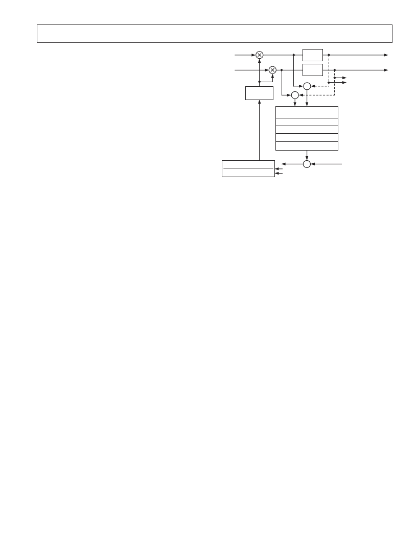
The AGC and the interpolation filters are not tied together and
any one, or both of them, can be selected without the other. The
AGC section can be bypassed, if desired, by setting Bit 0 of the
AGC control word. When bypassed, the I/Q data is still clipped
to a desired number of bits and a constant gain can be provided
through the AGC Gain multiplier.
There are three sources of error introduced by the AGC function:
underflow, overflow, and modulation. Underflow is caused by
truncation of bits below the output range. Overflow is caused by
clipping errors when the output signal exceeds the output
range. Modulation error occurs when the output gain varies
during the reception of data.
The desired signal level should be set based on the probability
density function of the signal so that the errors due to underflow
and overflow are balanced. The gain and damping values of the
loop filter should be set so that the AGC is fast enough to track
long-term amplitude variations of the signal that might cause
excessive underflow or overflow, but slow enough to avoid
excessive loss of amplitude information due to the modulation
of the signal.
The AGC Loop
The AGC loop is implemented using a log-linear architecture.
It contains four basic operations: power calculation, error calcu-
lation, loop filtering, and gain multiplication.
The AGC can be configured to operate in one of two modes:
Desired Signal level mode or Desired Clipping level mode as set
by Bit 4 of AGC control word (0x0A, 0x12). The AGC adjusts
the gain of the incoming data according to how far it is from a
given desired signal level or desired clipping level, depending on
the mode of operation selected. Two data paths to the AGC
loop are provided: one before the clipping circuitry and one
after the clipping circuitry, as shown in Figure 33. For Desired
Signal level mode, only the I/Q path from before the clipping is
used. For Desired Clipping level mode, the difference of the
I/Q signals from before and after the clipping circuitry is used.
Desired Signal Level Mode
In this mode of operation, the AGC strives to maintain the output
signal at a programmable set level. This mode of operation is
selected by putting a value of zero in Bit 4 of AGC control word
(0x0A, 0x12). First, the loop finds the square (or power) of the
incoming complex data signal by squaring I and Q and adding
them. This operation is implemented in exponential domain
using 2
x
(power of 2).
The AGC loop has an average and decimate block. This average
and decimate operation takes place on power samples and before
the square root operation. This block can be programmed to
average 1–16384 power samples and the decimate section can
be programmed to update the AGC once every 1–4096 samples.
The limitation on the averaging operation is that the number of
averaged power samples should be a multiple of the decimation
value (1 , 2 , 3 , or 4 times).
The averaging and decimation effectively means the AGC can
operate over averaged power of 1–16384 output samples. The
choice of updating the AGC once every 1–4096 samples and
operating on average power facilitates the implementation of
loop filter with slow time constants, where the AGC error con-
verges slowly and makes infrequent gain adjustments. It would
also be useful in scenarios where the user wants to keep the gain
scaling constant over a frame of data (or a stream of symbols).
CLIP
I
23 BITS
Q
CLIP
MEAN SQUARE (I+jQ)
AVERAGE 1–16384 SAMPLES
DECIMATE 1–4096 SAMPLES
SQUARE ROOT
USED ONLY FOR
DESIRED
CLIPPING LEVEL
MODE
GAIN
MULTIPLIER
I
Q
–
–
2
X
POWER OF 2
Kz
–1
1 – (1 + P)z
–1
+ Pz
–2
ERROR
'K' GAIN
'P' POLE
+
–
'R' DESIRED
PROGRAMMABLE
BIT WIDTH
LOG
2
(X)
Figure 33. Block Diagram of the AGC
Due to the limitation on the number of average samples to be a
multiple of decimation value, only the multiple number 1, 2, 3,
or 4 is programmed. This number is programmed in Bits 1,0 of
0x10 and 0x18 registers. These averaged samples are then deci-
mated with decimation ratios programmable from 1 to 4096. This
decimation ratio is defined in 12-bit registers 0x11 and 0x19.
The average and decimate operations are tied together and
implemented using a first-order CIC filter and some FIFO
registers. There is a gain and bit growth associated with CIC
filters and these depend on the decimation ratio. To compen-
sate for the gain associated with these operations, attenuation
scaling is provided before the CIC filter.
This scaling operation accounts for the division associated with
averaging operation as well as the traditional bit growth in CIC
filters. Since this scaling is implemented as a bit shift operation,
only coarse scaling is possible. Fine scale is implemented as an
offset in the request level explained later. The attenuation scaling
S
CIC
is programmable from 0 to 14 using four bits of 0x10 and
0x18 registers and is given by:
[
where,
M
CIC
is the decimation ratio (1–4096) and
N
AVG
is the
number of averaged samples programmed as a multiple of deci-
mation ratio (1, 2, 3, or 4).
For example, if a decimation ratio M
CIC
is 1000 and N
AVG
is
selected to be 3 (decimation of 1000 and averaging of 3000
samples), the actual gain due to averaging and decimation is 3000
or 69.54 dB ( = log
2
(3000)). Since attenuation is implemented
as a bit shift operation, only multiples of 6.02 dB attenuations
are possible. S
CIC
in this case is 12, corresponding to 72.24 dB.
This way, S
CIC
scaling always attenuates more than sufficient to
compensate for the gain changes in average and decimate sections
and thus prevents overflows in the AGC loop. It is also evident
that the CIC scaling is inducing a gain error (difference between
gain due to CIC and attenuation provided) of up to 6.02 dB.
This error should be compensated for in the request signal level as
explained below.
Logarithm to the base 2 is applied to the output from the average
and decimate section. These decimated power samples (in logarith-
mic domain) are converted to rms signal samples by applying a
square root. This square root is implemented using a simple shift
S
ceil
M
N
CIC
CIC
AVG
=
×
(
)
]
log
2
相关PDF资料 |
PDF描述 |
|---|---|
| AD6634PCB | 80 MSPS, Dual-Channel WCDMA Receive Signal Processor (RSP) |
| AD6635 | 4-Channel, 80 MSPS WCDMA Receive Signal Processor (RSP) |
| AD6635BB | 4-Channel, 80 MSPS WCDMA Receive Signal Processor (RSP) |
| AD6636 | 150 MSPS Wideband Digital Down-Converter (DDC) |
| AD6636BBCZ1 | 150 MSPS Wideband Digital Down-Converter (DDC) |
相关代理商/技术参数 |
参数描述 |
|---|---|
| AD6634BBCZ | 功能描述:IC RSP 80MSPS DUAL 196CSPBGA RoHS:是 类别:RF/IF 和 RFID >> RF 混频器 系列:AD6634 产品培训模块:Lead (SnPb) Finish for COTS Obsolescence Mitigation Program 标准包装:100 系列:- RF 型:W-CDMA 频率:2.11GHz ~ 2.17GHz 混频器数目:1 增益:17dB 噪音数据:2.2dB 次要属性:- 电流 - 电源:11.7mA 电源电压:2.7 V ~ 3.3 V 包装:托盘 封装/外壳:12-VFQFN 裸露焊盘 供应商设备封装:12-QFN-EP(3x3) |
| AD6634BC/PCB | 制造商:Analog Devices 功能描述:WCDMA RECEIVE SGNL PROCESSOR - Bulk |
| AD6634PCB | 制造商:AD 制造商全称:Analog Devices 功能描述:80 MSPS, Dual-Channel WCDMA Receive Signal Processor (RSP) |
| AD6635 | 制造商:AD 制造商全称:Analog Devices 功能描述:4-Channel, 80 MSPS WCDMA Receive Signal Processor (RSP) |
| AD6635BB | 功能描述:IC RSP 80MSPS QUAD 324-BGA RoHS:否 类别:RF/IF 和 RFID >> RF 混频器 系列:AD6635 产品培训模块:Lead (SnPb) Finish for COTS Obsolescence Mitigation Program 标准包装:100 系列:- RF 型:W-CDMA 频率:2.11GHz ~ 2.17GHz 混频器数目:1 增益:17dB 噪音数据:2.2dB 次要属性:- 电流 - 电源:11.7mA 电源电压:2.7 V ~ 3.3 V 包装:托盘 封装/外壳:12-VFQFN 裸露焊盘 供应商设备封装:12-QFN-EP(3x3) |
发布紧急采购,3分钟左右您将得到回复。