参数资料
| 型号: | AD9735BBCZ |
| 厂商: | Analog Devices Inc |
| 文件页数: | 30/72页 |
| 文件大小: | 0K |
| 描述: | IC DAC 12BIT 1.2GSPS 160-CSPBGA |
| 产品培训模块: | Data Converter Fundamentals DAC Architectures |
| 标准包装: | 1 |
| 位数: | 12 |
| 数据接口: | 并联 |
| 转换器数目: | 1 |
| 电压电源: | 模拟和数字 |
| 功率耗散(最大): | 550mW |
| 工作温度: | -40°C ~ 85°C |
| 安装类型: | 表面贴装 |
| 封装/外壳: | 160-LFBGA,CSPBGA |
| 供应商设备封装: | 160-CSPBGA(12x12) |
| 包装: | 托盘 |
| 输出数目和类型: | 2 电流,单极 |
| 采样率(每秒): | 1.2G |
第1页第2页第3页第4页第5页第6页第7页第8页第9页第10页第11页第12页第13页第14页第15页第16页第17页第18页第19页第20页第21页第22页第23页第24页第25页第26页第27页第28页第29页当前第30页第31页第32页第33页第34页第35页第36页第37页第38页第39页第40页第41页第42页第43页第44页第45页第46页第47页第48页第49页第50页第51页第52页第53页第54页第55页第56页第57页第58页第59页第60页第61页第62页第63页第64页第65页第66页第67页第68页第69页第70页第71页第72页
AD9734/AD9735/AD9736
Rev. A | Page 36 of 72
SERIAL PERIPHERAL INTERFACE
The AD973x serial port is a flexible, synchronous serial
communications port, allowing easy interface to many
industry-standard microcontrollers and microprocessors. The
serial I/O is compatible with most synchronous transfer
formats, including both the Motorola SPI and Intel SSR
protocols. The interface allows read/write access to all registers
that configure the AD973x. Single- or multiple-byte transfers
are supported, as well as most significant bit first (MSB-first) or
least significant bit first (LSB-first) transfer formats. The
AD973x serial interface port can be configured as a single pin
I/O (SDIO) or two unidirectional pins for in/out (SDIO/SDO).
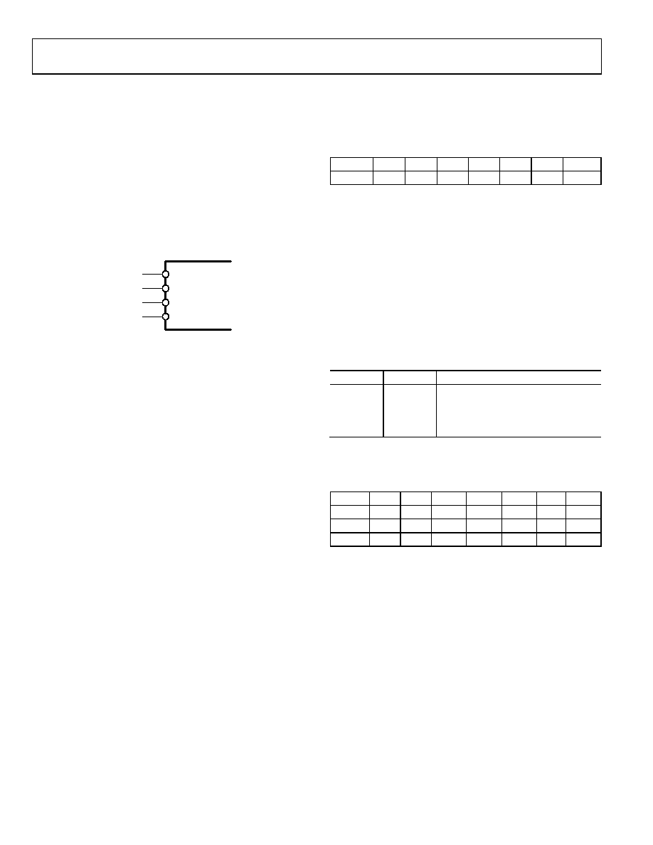
SDO (PIN G14)
SDIO (PIN F14)
SCLK (PIN G13)
CSB (PIN F13)
AD973x
SPI PORT
04862-066
Figure 68. AD973x SPI Port
The AD973x can optionally be configured via external pins
rather than the serial interface. When the PIN_MODE input
(Pin L1) is high, the serial interface is disabled and its pins are
reassigned for direct control of the DAC. Specific functionality
is described in the Pin Mode Operation section.
GENERAL OPERATION OF THE SERIAL INTERFACE
There are two phases to a communication cycle with the
AD973x. Phase 1 is the instruction cycle, which is the writing of
an instruction byte into the AD973x, coincident with the first
eight SCLK rising edges. The instruction byte provides the
AD973x serial port controller with information regarding the
data transfer cycle, which is Phase 2 of the communication
cycle. The Phase 1 instruction byte defines whether the
upcoming data transfer is read or write, the number of bytes in
the data transfer, and the starting register address for the first
byte of the data transfer. The first eight SCLK rising edges of
each communication cycle are used to write the instruction byte
into the AD973x.
The remaining SCLK edges are for Phase 2 of the communica-
tion cycle. Phase 2 is the actual data transfer between the
AD973x and the system controller. Phase 2 of the communica-
tion cycle is a transfer of 1, 2, 3, or 4 data bytes as determined
by the instruction byte. Using one multibyte transfer is the
preferred method. Single-byte data transfers are useful to
reduce CPU overhead when register access requires one byte
only. Registers change immediately upon writing to the last bit
of each transfer byte.
CSB (Chip Select) can be raised after each sequence of 8 bits
(except the last byte) to stall the bus. The serial transfer resumes
when CSB is lowered. Stalling on nonbyte boundaries resets
the SPI.
SHORT INSTRUCTION MODE (8-BIT INSTRUCTION)
The short instruction byte is shown in the following table:
MSB
LSB
I7
I6
I5
I4
I3
I2
I1
I0
R/W
N1
N0
A4
A3
A2
A1
A0
R/W, Bit 7 of the instruction byte, determines whether a read or
a write data transfer occurs after the instruction byte write.
Logic high indicates read operation. Logic 0 indicates a write
operation. N1, N0, Bit 6, and Bit 5 of the instruction byte
determine the number of bytes to be transferred during the data
transfer cycle. The bit decodes are shown in Table 20.
A4, A3, A2, A1, A0, Bit 4, Bit 3, Bit 2, Bit 1, and Bit 0 of the
instruction byte, determine which register is accessed during
the data transfer portion of the communications cycle. For
multibyte transfers, this address is the starting byte address. The
remaining register addresses are generated by the AD973x,
based on the LSBFIRST bit (Reg. 0, Bit 6).
Table 20. Byte Transfer Count
N1
N2
Description
0
Transfer 1 byte
0
1
Transfer 2 bytes
1
0
Transfer 3 bytes
1
Transfer 4 bytes
LONG INSTRUCTION MODE (16-BIT INSTRUCTION)
The long instruction bytes are shown in the following table:
MSB
LSB
I15
I14
I13
I12
I11
I10
I9
I8
R/W
N1
N0
A12
A11
A10
A9
A8
I7
I6
I5
I4
I3
I2
I1
I0
A7
A6
A5
A4
A3
A2
A1
A0
If LONG_INS = 1 (Reg. 0, Bit 4), the instruction byte is
extended to 2 bytes where the second byte provides an
additional 8 bits of address information. Address 0x00 to
Address 0x1F are equivalent in short and long instruction
modes. The AD973x does not use any addresses greater than 31
(0x1F), so always set LONG_INS = 0.
SERIAL INTERFACE PORT PIN DESCRIPTIONS
SCLK—Serial Clock
The serial clock pin is used to synchronize data to and from the
AD973x and to run the internal state machines. The maximum
frequency of SCLK is 20 MHz. All data input to the AD973x is
registered on the rising edge of SCLK. All data is driven out of
the AD973x on the rising edge of SCLK.
相关PDF资料 |
PDF描述 |
|---|---|
| AD7225LPZ | IC DAC 8BIT QUAD W/AMP 28-PLCC |
| AD9776BSVZ | IC DAC 12BIT DUAL 1GSPS 100TQFP |
| ADDAC80D-CBI-V | IC DAC 12BIT LOW COST 24-CDIP |
| AD7247KNZ | IC DAC 12BIT W/AMP W/BUFF 24-DIP |
| VI-2NW-IV-F1 | CONVERTER MOD DC/DC 5.5V 150W |
相关代理商/技术参数 |
参数描述 |
|---|---|
| AD9735BBCZ1 | 制造商:AD 制造商全称:Analog Devices 功能描述:10-/12-/14-Bit, 1200 MSPS DACS |
| AD9735BBCZRL | 功能描述:IC DAC 12BIT 1.2GSPS 160-CSPBGA RoHS:是 类别:集成电路 (IC) >> 数据采集 - 数模转换器 系列:- 产品培训模块:Data Converter Fundamentals DAC Architectures 标准包装:750 系列:- 设置时间:7µs 位数:16 数据接口:并联 转换器数目:1 电压电源:双 ± 功率耗散(最大):100mW 工作温度:0°C ~ 70°C 安装类型:表面贴装 封装/外壳:28-LCC(J 形引线) 供应商设备封装:28-PLCC(11.51x11.51) 包装:带卷 (TR) 输出数目和类型:1 电压,单极;1 电压,双极 采样率(每秒):143k |
| AD9735BBCZRL1 | 制造商:AD 制造商全称:Analog Devices 功能描述:10-/12-/14-Bit, 1200 MSPS DACS |
| AD9735-DPG2-EBZ | 功能描述:BOARD EVAL FOR AD9735 RoHS:是 类别:编程器,开发系统 >> 评估板 - 数模转换器 (DAC) 系列:* 产品培训模块:Lead (SnPb) Finish for COTS Obsolescence Mitigation Program 标准包装:1 系列:- DAC 的数量:4 位数:12 采样率(每秒):- 数据接口:串行,SPI? 设置时间:3µs DAC 型:电流/电压 工作温度:-40°C ~ 85°C 已供物品:板 已用 IC / 零件:MAX5581 |
| AD9735-EB | 制造商:Analog Devices 功能描述: |
发布紧急采购,3分钟左右您将得到回复。