参数资料
| 型号: | AD9735BBCZ |
| 厂商: | Analog Devices Inc |
| 文件页数: | 32/72页 |
| 文件大小: | 0K |
| 描述: | IC DAC 12BIT 1.2GSPS 160-CSPBGA |
| 产品培训模块: | Data Converter Fundamentals DAC Architectures |
| 标准包装: | 1 |
| 位数: | 12 |
| 数据接口: | 并联 |
| 转换器数目: | 1 |
| 电压电源: | 模拟和数字 |
| 功率耗散(最大): | 550mW |
| 工作温度: | -40°C ~ 85°C |
| 安装类型: | 表面贴装 |
| 封装/外壳: | 160-LFBGA,CSPBGA |
| 供应商设备封装: | 160-CSPBGA(12x12) |
| 包装: | 托盘 |
| 输出数目和类型: | 2 电流,单极 |
| 采样率(每秒): | 1.2G |
第1页第2页第3页第4页第5页第6页第7页第8页第9页第10页第11页第12页第13页第14页第15页第16页第17页第18页第19页第20页第21页第22页第23页第24页第25页第26页第27页第28页第29页第30页第31页当前第32页第33页第34页第35页第36页第37页第38页第39页第40页第41页第42页第43页第44页第45页第46页第47页第48页第49页第50页第51页第52页第53页第54页第55页第56页第57页第58页第59页第60页第61页第62页第63页第64页第65页第66页第67页第68页第69页第70页第71页第72页
AD9734/AD9735/AD9736
Rev. A | Page 38 of 72
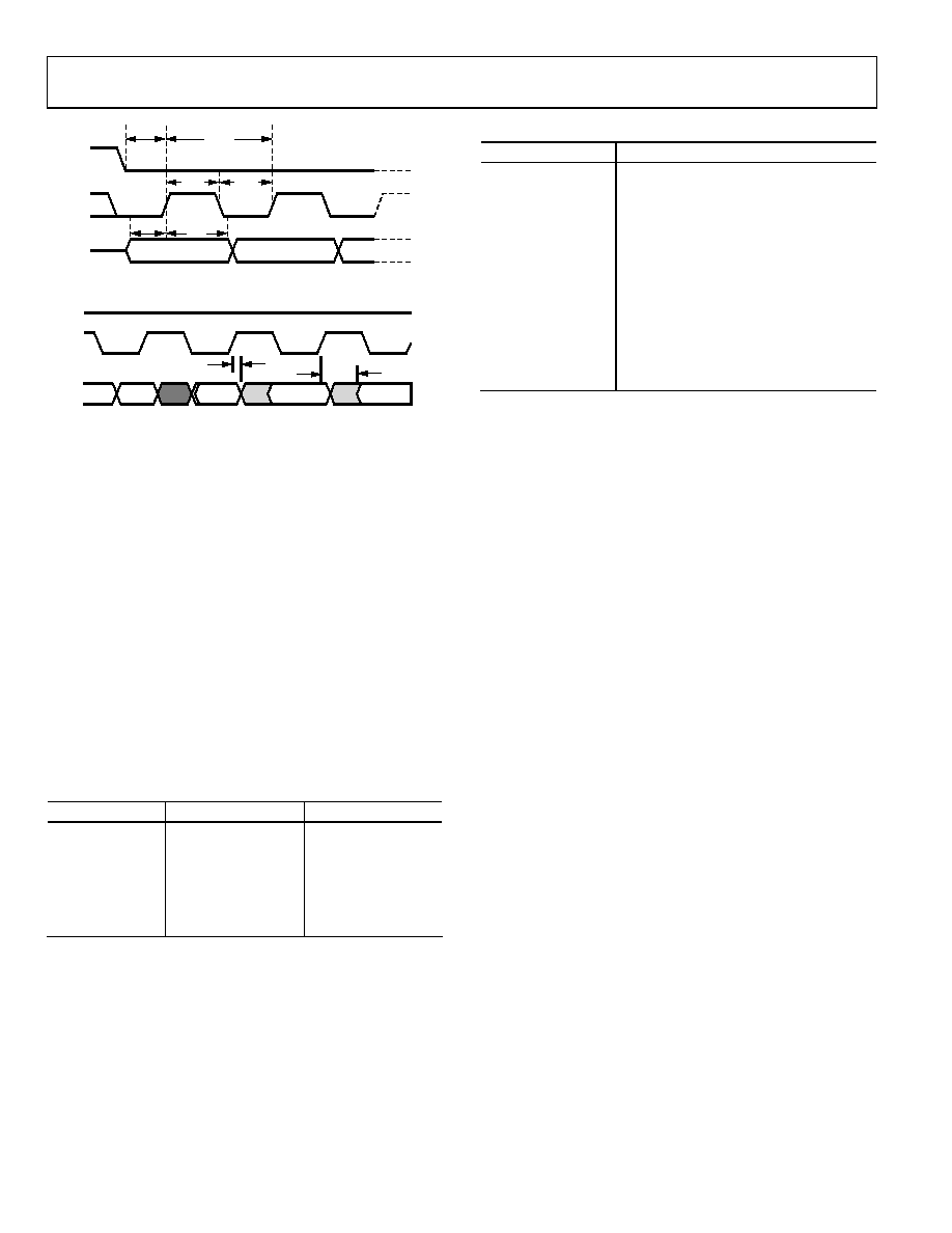
INSTRUCTION BIT 6
INSTRUCTION BIT 7
CSB
SCLK
SDIO
tDS
tDH
tPWH
tPWL
tSCLK
04862-071
Figure 73. Timing Diagram for SPI Register Write
I1
I0
D7
D6
D5
tDV
tDNV
CSB
SCLK
SDIO
04862-072
Figure 74. Timing Diagram for SPI Register Read
After the last instruction bit is written to the SDIO pin, the
driving signal must be set to a high impedance in time for the
bus to turn around. The serial output data from the AD973x is
enabled by the falling edge of SCLK. This causes the first output
data bit to be shorter than the remaining data bits, as shown in
To assure proper reading of data, read the SDIO or SDO pin
prior to changing the SCLK from low to high. Due to the more
complex multibyte protocol, multiple AD973x devices cannot
be daisy-chained on the SPI bus. Multiple DACs should be
controlled by independent CSB signals.
PIN MODE OPERATION
When the PIN_MODE input (Pin L1) is set high, the SPI port is
disabled. The SPI port pins are remapped, as shown in Table 21.
The function of these pins is described in Table 22. The remain-
ing PIN_MODE register settings are shown in Table 9.
Table 21. SPI_MODE vs. PIN_MODE Inputs
Pin Number
PIN_MODE = 0
PIN_MODE = 1
E13
IRQ
UNSIGNED
F13
CSB
2×
G13
SCLK
FSC0
E14
RESET
PD
F14
SDIO
FIFO
G14
SDO
FSC1
Table 22. PIN_MODE Input Functions
Mnemonic
Function
UNSIGNED
0, twos complement input data format
1, unsigned input data format
2×
0, interpolation disabled
1, interpolation = 2× enabled
FSC1, FSC0
00, sleep mode
01, 10 mA full-scale output current
10, 20 mA full-scale output current
11, 30 mA full-scale output current
PD
0, chip enabled
1, chip in power-down state
FIFO
0, input FIFO disabled
1, input FIFO enabled
Care must be taken when using PIN_MODE because only the
control bits shown in Table 22 can be changed. If the remaining
register default values are not suitable for the desired operation,
PIN_MODE cannot be used. If the FIFO is enabled, the
controller clock must be less than 10 MHz. This limits the DAC
clock to 160 MHz.
RESET OPERATION
The RESET pin forces all SPI register contents to their default
values (see Table 9), which places the DAC in a known state.
The software reset bit forces all SPI register contents, except
Reg. 0 and Reg. 4, to their default values.
The internal reset signal is derived from a logical OR operation
on the RESET pin state and from the software reset state. This
internal reset signal drives all SPI registers to their default
values, except Reg. 0 and Reg. 4, which are unaffected. The data
registers are not affected by either reset.
The software reset is asserted by writing 1 to Reg. 0, Bit 5. It
may be cleared on the next SPI write cycle or a later write cycle.
PROGRAMMING SEQUENCE
The AD973x registers should be programmed in this order:
1.
Reset hardware.
2.
Make changes to SPI port configuration, if necessary.
3.
Input format, if unsigned.
4.
Interpolation, if in 2× mode.
5.
Calibrate and set the LVDS controller.
6.
Enable the FIFO.
7.
Calibrate and set the sync controller.
Step 1 through Step 4 are required, while Step 5 through Step 7
are optional. The LVDS controller can help assure proper data
reception in the DAC with changes in temperature and voltage.
The sync controller manages the FIFO to assure proper transfer
of the received data to the DAC core with changes in
temperature and voltage. The DAC is intended to operate with
both controllers active unless data and clock alignment is
managed externally.
相关PDF资料 |
PDF描述 |
|---|---|
| AD7225LPZ | IC DAC 8BIT QUAD W/AMP 28-PLCC |
| AD9776BSVZ | IC DAC 12BIT DUAL 1GSPS 100TQFP |
| ADDAC80D-CBI-V | IC DAC 12BIT LOW COST 24-CDIP |
| AD7247KNZ | IC DAC 12BIT W/AMP W/BUFF 24-DIP |
| VI-2NW-IV-F1 | CONVERTER MOD DC/DC 5.5V 150W |
相关代理商/技术参数 |
参数描述 |
|---|---|
| AD9735BBCZ1 | 制造商:AD 制造商全称:Analog Devices 功能描述:10-/12-/14-Bit, 1200 MSPS DACS |
| AD9735BBCZRL | 功能描述:IC DAC 12BIT 1.2GSPS 160-CSPBGA RoHS:是 类别:集成电路 (IC) >> 数据采集 - 数模转换器 系列:- 产品培训模块:Data Converter Fundamentals DAC Architectures 标准包装:750 系列:- 设置时间:7µs 位数:16 数据接口:并联 转换器数目:1 电压电源:双 ± 功率耗散(最大):100mW 工作温度:0°C ~ 70°C 安装类型:表面贴装 封装/外壳:28-LCC(J 形引线) 供应商设备封装:28-PLCC(11.51x11.51) 包装:带卷 (TR) 输出数目和类型:1 电压,单极;1 电压,双极 采样率(每秒):143k |
| AD9735BBCZRL1 | 制造商:AD 制造商全称:Analog Devices 功能描述:10-/12-/14-Bit, 1200 MSPS DACS |
| AD9735-DPG2-EBZ | 功能描述:BOARD EVAL FOR AD9735 RoHS:是 类别:编程器,开发系统 >> 评估板 - 数模转换器 (DAC) 系列:* 产品培训模块:Lead (SnPb) Finish for COTS Obsolescence Mitigation Program 标准包装:1 系列:- DAC 的数量:4 位数:12 采样率(每秒):- 数据接口:串行,SPI? 设置时间:3µs DAC 型:电流/电压 工作温度:-40°C ~ 85°C 已供物品:板 已用 IC / 零件:MAX5581 |
| AD9735-EB | 制造商:Analog Devices 功能描述: |
发布紧急采购,3分钟左右您将得到回复。