参数资料
| 型号: | AD9735BBCZ |
| 厂商: | Analog Devices Inc |
| 文件页数: | 51/72页 |
| 文件大小: | 0K |
| 描述: | IC DAC 12BIT 1.2GSPS 160-CSPBGA |
| 产品培训模块: | Data Converter Fundamentals DAC Architectures |
| 标准包装: | 1 |
| 位数: | 12 |
| 数据接口: | 并联 |
| 转换器数目: | 1 |
| 电压电源: | 模拟和数字 |
| 功率耗散(最大): | 550mW |
| 工作温度: | -40°C ~ 85°C |
| 安装类型: | 表面贴装 |
| 封装/外壳: | 160-LFBGA,CSPBGA |
| 供应商设备封装: | 160-CSPBGA(12x12) |
| 包装: | 托盘 |
| 输出数目和类型: | 2 电流,单极 |
| 采样率(每秒): | 1.2G |
第1页第2页第3页第4页第5页第6页第7页第8页第9页第10页第11页第12页第13页第14页第15页第16页第17页第18页第19页第20页第21页第22页第23页第24页第25页第26页第27页第28页第29页第30页第31页第32页第33页第34页第35页第36页第37页第38页第39页第40页第41页第42页第43页第44页第45页第46页第47页第48页第49页第50页当前第51页第52页第53页第54页第55页第56页第57页第58页第59页第60页第61页第62页第63页第64页第65页第66页第67页第68页第69页第70页第71页第72页
AD9734/AD9735/AD9736
Rev. A | Page 55 of 72
SYNCHRONIZATION TIMING
When more than one AD973x must be synchronized or when
a constant group delay must be maintained, the internal
controllers cannot be used. If the FIFO is enabled, the delay
between multiple AD973x devices is unknown. If the
DATACLK_OUT from multiple devices is used, there is an
uncertainty of two DACCLK periods because the initial phase
of DATACLK_OUT with respect to DACCLK cannot be
controlled. This means one DAC must be used to provide
DATACLK_OUT for all synchronized DACs and all timing
must be externally managed. The following timing information
allows system timing to be calculated so that multiple AD973xs
can be synchronized.
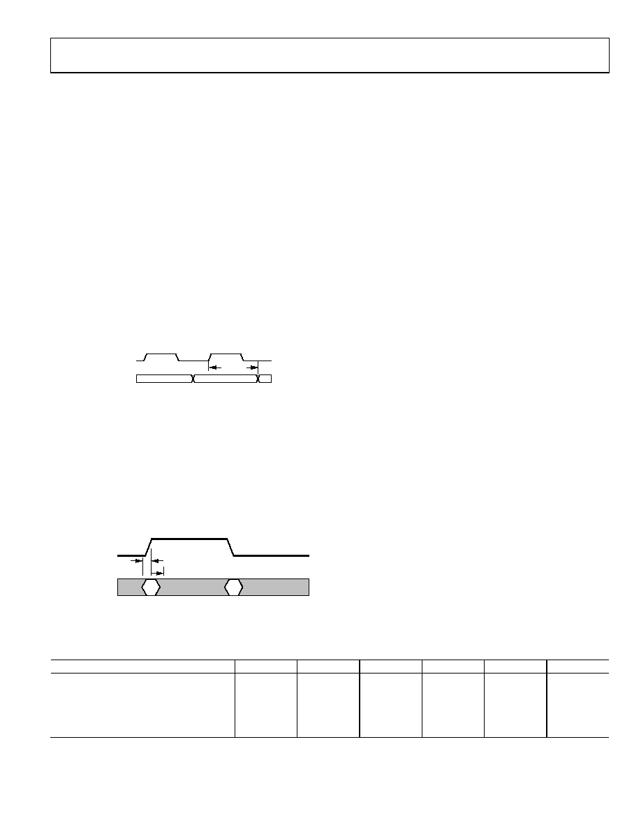
DATACLK_OUT changes relative to the rising edge of
DACCLK+ and is delayed, as shown in Figure 101. Because
DACCLK is divided by 2 to create DATACLK_OUT, the phase
of DATACLK_OUT can be 0° or 180°. There is no way to
predict or control this relationship. It can be different after each
power cycle and is not affected by hardware or software resets.
tDDCO
DACCLK
DATACLK_OUT
04862-099
Figure 101. DACCLK to DATACLK_OUT Delay
The incoming data is de-interleaved internally as shown in
Figure 78. In Figure 78, DBU (upper) and DBL (lower) represent
the de-interleaved data paths. Each edge of DATACLK_IN
latches an incoming sample in two alternating registers. The
DATACLK_IN to data setup and hold definitions are illustrated
in Figure 102. All the data input must be valid during the setup-
and-hold period. External skew effectively increases the setup
and hold times that the data source must meet.
04862-
100
DATACLK_IN
OR DATACLK_OUT
DATA_IN
tDH
tDSU
Figure 102. Standard Definitions for DATACLK_IN or DATACLK_OUT to
Data Setup and Hold, SD = 0
While correct DATA_IN vs. DATACLK_IN timing is critical,
the transition of the incoming data to the DACCLK domain is
equally critical. By referencing the incoming DATA and
DATACLK_IN timing to the DATACLK_OUT signal, some
timing uncertainty can be removed. The DATACLK_OUT
timing very closely tracks the timing of the DACCLK-
controlled registers. Any variation in the path delay affects both
paths in almost the same way. If DATACLK_OUT is not used,
the full DACCLK to DATACLK_OUT path variation reduces
the external timing margin. Figure 101 shows a simplified view
of the internal clocking scheme with the relevant delay paths.
The internal architecture is interleaved such that each phase has
twice as long to make the transition across the clock domains.
This results in an extremely narrow window where the
incoming data must be held stable.
Table 28 shows the timing parameters for Figure 101 and
Figure 102. These parameters were measured for a sample of
five devices from five silicon lots. Worst-case fast and slow skew
lots were included in addition to the nominal (or average) lot.
The typical 40°C to typical +85°C spread illustrates the
variability with temperature for a single lot. Adding in lot-to-lot
variation with the fast and slow lots indicates the worst-case
spread in timing.
The timing varies such that all of the parameters move in the
same direction. For example, if the DATACLK_IN to data setup
time is fast, the hold time is similarly fast. The DACCLK to
DATACLK_OUT delay and the DATACLK_OUT to data setup
and hold is also at the fast end of the range.
Note that the polarities of setup-and-hold values in Table 28
conform to the standard convention of setup time occurring
prior to the latching edge and hold time occurring after the
latching edge, as shown in Figure 102.
Table 28. AD973x Clock and Data Timing Parameters
Symbol and Definition
Fast 40°C
Typ 40°C
All +25°C
Typ +85°C
Slow +85°C
Unit
tDDCO DACCLK to DATACLK_OUT Delay
+1650
+1800
+1890
+2050
+2350
ps
tDCISU DATACLK_IN to DATA Setup
100
120
150
170
220
ps
tDCIH DATACLK_IN to DATA Hold
+210
+220
+240
+280
+360
ps
tDISU DATACLK_OUT to DATA Setup
+1310
+1440
+1611
+1710
+1970
ps
tDIH DATACLK_OUT to DATA Hold
1250
1360
1548
1640
1890
ps
相关PDF资料 |
PDF描述 |
|---|---|
| AD7225LPZ | IC DAC 8BIT QUAD W/AMP 28-PLCC |
| AD9776BSVZ | IC DAC 12BIT DUAL 1GSPS 100TQFP |
| ADDAC80D-CBI-V | IC DAC 12BIT LOW COST 24-CDIP |
| AD7247KNZ | IC DAC 12BIT W/AMP W/BUFF 24-DIP |
| VI-2NW-IV-F1 | CONVERTER MOD DC/DC 5.5V 150W |
相关代理商/技术参数 |
参数描述 |
|---|---|
| AD9735BBCZ1 | 制造商:AD 制造商全称:Analog Devices 功能描述:10-/12-/14-Bit, 1200 MSPS DACS |
| AD9735BBCZRL | 功能描述:IC DAC 12BIT 1.2GSPS 160-CSPBGA RoHS:是 类别:集成电路 (IC) >> 数据采集 - 数模转换器 系列:- 产品培训模块:Data Converter Fundamentals DAC Architectures 标准包装:750 系列:- 设置时间:7µs 位数:16 数据接口:并联 转换器数目:1 电压电源:双 ± 功率耗散(最大):100mW 工作温度:0°C ~ 70°C 安装类型:表面贴装 封装/外壳:28-LCC(J 形引线) 供应商设备封装:28-PLCC(11.51x11.51) 包装:带卷 (TR) 输出数目和类型:1 电压,单极;1 电压,双极 采样率(每秒):143k |
| AD9735BBCZRL1 | 制造商:AD 制造商全称:Analog Devices 功能描述:10-/12-/14-Bit, 1200 MSPS DACS |
| AD9735-DPG2-EBZ | 功能描述:BOARD EVAL FOR AD9735 RoHS:是 类别:编程器,开发系统 >> 评估板 - 数模转换器 (DAC) 系列:* 产品培训模块:Lead (SnPb) Finish for COTS Obsolescence Mitigation Program 标准包装:1 系列:- DAC 的数量:4 位数:12 采样率(每秒):- 数据接口:串行,SPI? 设置时间:3µs DAC 型:电流/电压 工作温度:-40°C ~ 85°C 已供物品:板 已用 IC / 零件:MAX5581 |
| AD9735-EB | 制造商:Analog Devices 功能描述: |
发布紧急采购,3分钟左右您将得到回复。