参数资料
| 型号: | AD9735BBCZ |
| 厂商: | Analog Devices Inc |
| 文件页数: | 37/72页 |
| 文件大小: | 0K |
| 描述: | IC DAC 12BIT 1.2GSPS 160-CSPBGA |
| 产品培训模块: | Data Converter Fundamentals DAC Architectures |
| 标准包装: | 1 |
| 位数: | 12 |
| 数据接口: | 并联 |
| 转换器数目: | 1 |
| 电压电源: | 模拟和数字 |
| 功率耗散(最大): | 550mW |
| 工作温度: | -40°C ~ 85°C |
| 安装类型: | 表面贴装 |
| 封装/外壳: | 160-LFBGA,CSPBGA |
| 供应商设备封装: | 160-CSPBGA(12x12) |
| 包装: | 托盘 |
| 输出数目和类型: | 2 电流,单极 |
| 采样率(每秒): | 1.2G |
第1页第2页第3页第4页第5页第6页第7页第8页第9页第10页第11页第12页第13页第14页第15页第16页第17页第18页第19页第20页第21页第22页第23页第24页第25页第26页第27页第28页第29页第30页第31页第32页第33页第34页第35页第36页当前第37页第38页第39页第40页第41页第42页第43页第44页第45页第46页第47页第48页第49页第50页第51页第52页第53页第54页第55页第56页第57页第58页第59页第60页第61页第62页第63页第64页第65页第66页第67页第68页第69页第70页第71页第72页
AD9734/AD9735/AD9736
Rev. A | Page 42 of 72
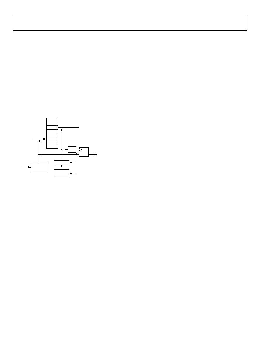
SYNC LOGIC AND CONTROLLER
A FIFO structure is utilized to synchronize the data transfer
between the DACCLK and the DATACLK_IN clock domains.
The sync controller writes data from DB<13:0> into an 8-word
memory register based on a cyclic write counter clocked by the
DSS, which is a delayed version of DACCLK_IN. The data is
read out of the memory based on a second cyclic read counter
clocked by DACCLK. The 8-word FIFO shown in Figure 82
provides sufficient margin to maintain proper timing under
most conditions. The sync logic is designed to prevent the read
and write pointers from crossing. If the timing drifts far enough
to require an update of the phase offset (PHOF<1:0>), two
samples are duplicated or dropped. Figure 83 shows the timing
diagram for the sync logic.
8 WORD
MEMORY
READ
COUNTER
PHOF<1:0>
DACCLK
FIFOSTAT<2:0>
DSS
M0
M7
ZD
DAC<13:0>
ADDER
WRITE
COUNTER
FF
DAC<13:0>
04862-080
Figure 82. Sync Logic Block Diagram
SYNC LOGIC AND CONTROLLER OPERATION
The relationship between the readout pointer and the write
pointer initially is unknown because the startup relationship
between DACCLK and DATACLK_IN is unknown. The sync
logic measures the relative phase between the two counters with
the zero detect block and the flip-flop in Figure 82. The relative
phase is returned in FIFOSTAT<2:0> (Reg. 7, Bits 6:4), and sync
logic errors are indicated by FIFOSTAT<3> (Reg. 7, Bit 7). If
FIFOSTAT<2:0> returns a value of 0 or 7, the memory is
sampling in a critical state (read and write pointers are close to
crossing).
If the FIFOSTAT<2:0> returns a value of 3 or 4, the memory is
sampling at the optimal state (read and write pointers are
farthest apart). If FIFOSTAT<2:0> returns a critical value, the
pointer can be adjusted with the phase offset PHOF<1:0> (Reg.
7, Bits 1:0). Due to the architecture of the FIFO, the phase offset
can only adjust the read pointer in steps of 2.
OPERATION IN MANUAL MODE
To start operating the DAC in manual mode, allow DACCLK
and DATACLK_IN to stabilize, then enable FIFO mode (Reg. 0,
Bit 2). Read FIFOSTAT<2:0> (Reg. 7, Bits 6:4) to determine if
adjustment is needed. For example, if FIFOSTAT<2:0> = 6, the
timing is not yet critical, but it is not optimal.
To return to an optimal state (FIFOSTAT<2:0> = 4), the
PHOF<1:0> (Reg. 7, Bits 1:0) needs to be set to 1. Setting
PHOF<1:0> = 1 effectively increments the read pointer by 2.
This causes the write pointer value to be captured two clocks
later, decreasing FIFOSTAT<2:0> from 6 to 4.
OPERATION IN SURVEILLANCE AND AUTO MODES
Once FIFOSTAT<2:0> is manually placed in an optimal state,
the AD973x sync logic can run in surveillance or auto mode. To
start, turn on surveillance mode by setting SSURV = 1 (Reg. 8,
Bit 7), then enable the sync interrupt (Reg. 1, Bit 2).
If STRH<0> = 0 (Reg. 8, Bit 0), an interrupt occurs if
FIFOSTAT<2:0> = 0 or 7. If STRH<0> = 1 (Reg. 8, Bit 0), an
interrupt occurs if FIFOSTAT<2:0> = 0, 1, 6, or 7. The interrupt
is read at Reg. 1, Bit 6 at the AD973x IRQ pin.
To enter auto mode, complete the preceding steps then set
SAUTO = 1 (Reg. 8, Bit 6). Next, set the sync interrupt = 0
(Reg. 1, Bit 2), to allow the phase offset (PHOF<1:0>) to be
automatically updated if FIFOSTAT<2:0> violates the threshold
value. The FIFOSTAT signal is filtered to improve noise
immunity and reduce unnecessary phase offset updates. The
filter operates with the following algorithm:
FIFOSTAT = FIFOSTAT + ΔFIFOSTAT/2 ^ SFLT<3:0>
where:
0 ≤ SFLT<3:0> ≤ 12
Values greater than 12 are set to 12. If SFLT<3:0> is too small,
clock jitter and noise can cause erratic behavior. Normally, SFLT
can be set to the maximum value.
FIFO BYPASS
When the FIFO_MODE bit (Reg. 1, Bit 2) is set to 0, the FIFO
is bypassed with a mux. When the FIFO is enabled, the pipeline
delay through the AD973x increases by the delta between the
FIFO read pointer and write pointer plus 4 more clock periods.
相关PDF资料 |
PDF描述 |
|---|---|
| AD7225LPZ | IC DAC 8BIT QUAD W/AMP 28-PLCC |
| AD9776BSVZ | IC DAC 12BIT DUAL 1GSPS 100TQFP |
| ADDAC80D-CBI-V | IC DAC 12BIT LOW COST 24-CDIP |
| AD7247KNZ | IC DAC 12BIT W/AMP W/BUFF 24-DIP |
| VI-2NW-IV-F1 | CONVERTER MOD DC/DC 5.5V 150W |
相关代理商/技术参数 |
参数描述 |
|---|---|
| AD9735BBCZ1 | 制造商:AD 制造商全称:Analog Devices 功能描述:10-/12-/14-Bit, 1200 MSPS DACS |
| AD9735BBCZRL | 功能描述:IC DAC 12BIT 1.2GSPS 160-CSPBGA RoHS:是 类别:集成电路 (IC) >> 数据采集 - 数模转换器 系列:- 产品培训模块:Data Converter Fundamentals DAC Architectures 标准包装:750 系列:- 设置时间:7µs 位数:16 数据接口:并联 转换器数目:1 电压电源:双 ± 功率耗散(最大):100mW 工作温度:0°C ~ 70°C 安装类型:表面贴装 封装/外壳:28-LCC(J 形引线) 供应商设备封装:28-PLCC(11.51x11.51) 包装:带卷 (TR) 输出数目和类型:1 电压,单极;1 电压,双极 采样率(每秒):143k |
| AD9735BBCZRL1 | 制造商:AD 制造商全称:Analog Devices 功能描述:10-/12-/14-Bit, 1200 MSPS DACS |
| AD9735-DPG2-EBZ | 功能描述:BOARD EVAL FOR AD9735 RoHS:是 类别:编程器,开发系统 >> 评估板 - 数模转换器 (DAC) 系列:* 产品培训模块:Lead (SnPb) Finish for COTS Obsolescence Mitigation Program 标准包装:1 系列:- DAC 的数量:4 位数:12 采样率(每秒):- 数据接口:串行,SPI? 设置时间:3µs DAC 型:电流/电压 工作温度:-40°C ~ 85°C 已供物品:板 已用 IC / 零件:MAX5581 |
| AD9735-EB | 制造商:Analog Devices 功能描述: |
发布紧急采购,3分钟左右您将得到回复。