参数资料
| 型号: | AD9735BBCZ |
| 厂商: | Analog Devices Inc |
| 文件页数: | 49/72页 |
| 文件大小: | 0K |
| 描述: | IC DAC 12BIT 1.2GSPS 160-CSPBGA |
| 产品培训模块: | Data Converter Fundamentals DAC Architectures |
| 标准包装: | 1 |
| 位数: | 12 |
| 数据接口: | 并联 |
| 转换器数目: | 1 |
| 电压电源: | 模拟和数字 |
| 功率耗散(最大): | 550mW |
| 工作温度: | -40°C ~ 85°C |
| 安装类型: | 表面贴装 |
| 封装/外壳: | 160-LFBGA,CSPBGA |
| 供应商设备封装: | 160-CSPBGA(12x12) |
| 包装: | 托盘 |
| 输出数目和类型: | 2 电流,单极 |
| 采样率(每秒): | 1.2G |
第1页第2页第3页第4页第5页第6页第7页第8页第9页第10页第11页第12页第13页第14页第15页第16页第17页第18页第19页第20页第21页第22页第23页第24页第25页第26页第27页第28页第29页第30页第31页第32页第33页第34页第35页第36页第37页第38页第39页第40页第41页第42页第43页第44页第45页第46页第47页第48页当前第49页第50页第51页第52页第53页第54页第55页第56页第57页第58页第59页第60页第61页第62页第63页第64页第65页第66页第67页第68页第69页第70页第71页第72页
AD9734/AD9735/AD9736
Rev. A | Page 53 of 72
DAC DATA SOURCES
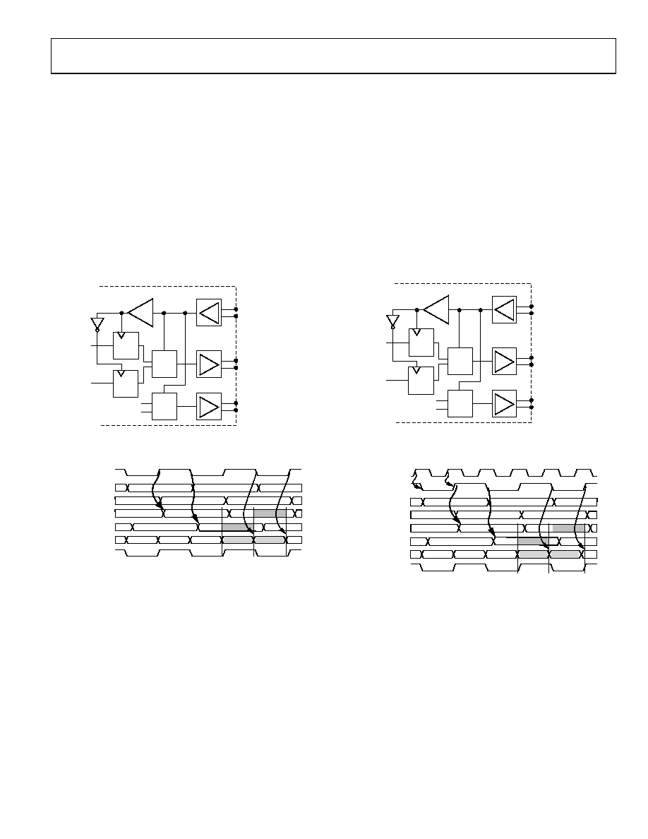
The circuit shown in Figure 96 allows optimum data alignment
when running the AD973x at full speed. This circuit can be
easily implemented in the FPGA or ASIC used to drive the
digital input. It is important to use the DATACLK_OUT signal
because it helps to cancel some of the timing errors. In this
configuration, DATACLK_OUT generates the DDR LVDS
DATACLK_IN to drive the AD973x. The circuit aligns the
DATACLK_IN and the digital input data (DB<13:0>) as
required by the AD973x. The LVDS controller in the AD973x
uses DATACLK_IN to generate the internal DSS to capture the
incoming data in the center of the valid data window.
04862-094
MUX
D1
DATACLK_OUT
FROM AD9736 (DDR)
DATACLK_IN
TO AD9736 (DDR)
DB(13:0) TO AD9736
DATA SOURCE
LOGIC 0
LOGIC 1
DATA2
DATA1
D2
Figure 96. Recommended FPGA/ASIC Configuration for Driving AD9736
Digital Inputs, 1× Mode
04862-095
DATA1
DATA2
AC
E
B
AB
C
D
B
D
D1
D2
DB
DATACLK_OUT+
DATACLK_IN+
Figure 97. FPGA/ASIC Timing for Driving AD973x Digital Inputs, 1× Mode
To operate in 2× mode, the circuit in Figure 96 must be
modified to include a divide-by-2 block in the path of
DATACLK_OUT. Without this additional divider, the data and
DATACLK_IN runs 2× too fast. DATACLK_OUT is always
DACCLK/2.
Contact FPGA vendors directly regarding the maximum output
data rates supported by their products.
04862-096
MUX
D1
DATACLK_OUT
FROM AD9736 (DDR)
DATACLK_IN
TO AD9736 (DDR)
DB(13:0) TO AD9736
DATA SOURCE
LOGIC 1
LOGIC 0
DATA2
DATA1
D2
÷2
Figure 98. Recommended FPGA/ASIC Configuration for Driving AD9736
Digital Inputs, 2× Mode
04862-097
CLK_OUT+/2
DATA2
DATA1
AC
E
B
AB
C
D
B
D
D1
D2
DB
DATACLK_OUT+
DATACLK_IN+
Figure 99. FPGA/ASIC Timing for Driving AD973x Digital Inputs, 2× Mode
相关PDF资料 |
PDF描述 |
|---|---|
| AD7225LPZ | IC DAC 8BIT QUAD W/AMP 28-PLCC |
| AD9776BSVZ | IC DAC 12BIT DUAL 1GSPS 100TQFP |
| ADDAC80D-CBI-V | IC DAC 12BIT LOW COST 24-CDIP |
| AD7247KNZ | IC DAC 12BIT W/AMP W/BUFF 24-DIP |
| VI-2NW-IV-F1 | CONVERTER MOD DC/DC 5.5V 150W |
相关代理商/技术参数 |
参数描述 |
|---|---|
| AD9735BBCZ1 | 制造商:AD 制造商全称:Analog Devices 功能描述:10-/12-/14-Bit, 1200 MSPS DACS |
| AD9735BBCZRL | 功能描述:IC DAC 12BIT 1.2GSPS 160-CSPBGA RoHS:是 类别:集成电路 (IC) >> 数据采集 - 数模转换器 系列:- 产品培训模块:Data Converter Fundamentals DAC Architectures 标准包装:750 系列:- 设置时间:7µs 位数:16 数据接口:并联 转换器数目:1 电压电源:双 ± 功率耗散(最大):100mW 工作温度:0°C ~ 70°C 安装类型:表面贴装 封装/外壳:28-LCC(J 形引线) 供应商设备封装:28-PLCC(11.51x11.51) 包装:带卷 (TR) 输出数目和类型:1 电压,单极;1 电压,双极 采样率(每秒):143k |
| AD9735BBCZRL1 | 制造商:AD 制造商全称:Analog Devices 功能描述:10-/12-/14-Bit, 1200 MSPS DACS |
| AD9735-DPG2-EBZ | 功能描述:BOARD EVAL FOR AD9735 RoHS:是 类别:编程器,开发系统 >> 评估板 - 数模转换器 (DAC) 系列:* 产品培训模块:Lead (SnPb) Finish for COTS Obsolescence Mitigation Program 标准包装:1 系列:- DAC 的数量:4 位数:12 采样率(每秒):- 数据接口:串行,SPI? 设置时间:3µs DAC 型:电流/电压 工作温度:-40°C ~ 85°C 已供物品:板 已用 IC / 零件:MAX5581 |
| AD9735-EB | 制造商:Analog Devices 功能描述: |
发布紧急采购,3分钟左右您将得到回复。