参数资料
| 型号: | AD9735BBCZ |
| 厂商: | Analog Devices Inc |
| 文件页数: | 33/72页 |
| 文件大小: | 0K |
| 描述: | IC DAC 12BIT 1.2GSPS 160-CSPBGA |
| 产品培训模块: | Data Converter Fundamentals DAC Architectures |
| 标准包装: | 1 |
| 位数: | 12 |
| 数据接口: | 并联 |
| 转换器数目: | 1 |
| 电压电源: | 模拟和数字 |
| 功率耗散(最大): | 550mW |
| 工作温度: | -40°C ~ 85°C |
| 安装类型: | 表面贴装 |
| 封装/外壳: | 160-LFBGA,CSPBGA |
| 供应商设备封装: | 160-CSPBGA(12x12) |
| 包装: | 托盘 |
| 输出数目和类型: | 2 电流,单极 |
| 采样率(每秒): | 1.2G |
第1页第2页第3页第4页第5页第6页第7页第8页第9页第10页第11页第12页第13页第14页第15页第16页第17页第18页第19页第20页第21页第22页第23页第24页第25页第26页第27页第28页第29页第30页第31页第32页当前第33页第34页第35页第36页第37页第38页第39页第40页第41页第42页第43页第44页第45页第46页第47页第48页第49页第50页第51页第52页第53页第54页第55页第56页第57页第58页第59页第60页第61页第62页第63页第64页第65页第66页第67页第68页第69页第70页第71页第72页
AD9734/AD9735/AD9736
Rev. A | Page 39 of 72
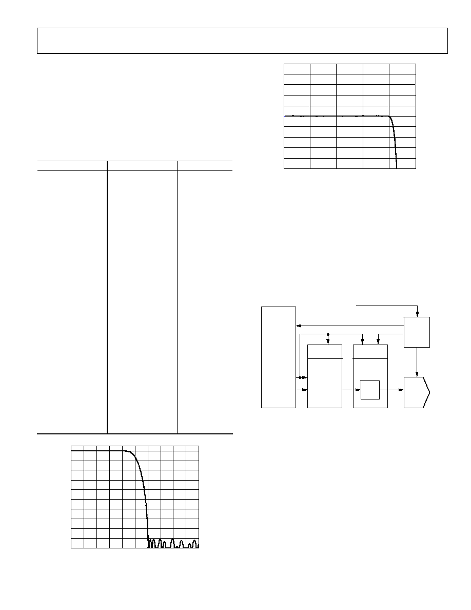
INTERPOLATION FILTER
In 2× mode, the input data is interpolated by a factor of 2 so
that it aligns with the DAC update rate. The interpolation filter
is a hard-coded, 55-tap, symmetric FIR with a 0.001 dB pass-
band flatness and a stop-band attenuation of about 90 dB. The
transition band runs from 20% of fDAC to 30% of fDAC. The FIR
response is shown in Figure 75 where the frequency axis is
Table 23 shows the 16-bit filter coefficients.
Table 23. FIR Interpolation Filter Coefficients
Coefficient Number
Tap Weight
1
55
7
2
54
0
3
53
+24
4
52
0
5
51
62
6
50
0
7
49
+135
8
48
0
9
47
263
10
46
0
11
45
+471
12
44
0
13
43
793
14
42
0
15
41
+1273
16
40
0
17
39
1976
18
38
0
19
37
+3012
20
36
0
21
35
4603
22
34
0
23
33
+7321
24
32
0
25
31
13270
26
30
0
27
29
+41505
28
+65535
04862-073
FREQUENCY NORMALIZED TO
fDAC
0.50
0
0.05 0.10 0.15 0.20 0.25 0.30 0.35 0.40 0.45
MAGNIT
UDE
(d
B)
0
–10
–20
–30
–40
–50
–60
–70
–80
–90
–100
Figure 75. Interpolation Filter Response
04862-074
FREQUENCY NORMALIZED TO
fDAC
0.25
0
0.10
0.05
0.15
0.20
MA
GN
ITU
D
E
(
d
B
)
0.10
0.06
0.08
0.02
–0.02
–0.06
0.04
0
–0.04
–0.08
–0.10
Figure 76. Interpolation Filter Pass-Band Flatness
DATA INTERFACE CONTROLLERS
Two internal controllers are utilized in the operation of the
AD973x. The first controller helps maintain optimum LVDS
data sampling; the second controller helps maintain optimum
synchronization between the DACCLK and the incoming data.
The LVDS controller is responsible for optimizing the sampling
of the data from the LVDS bus (DB13:0), while the sync
controller resolves timing problems between the DAC_CLK
(CLK+, CLK) and the DATACLK. A block diagram of these
controllers is shown in Figure 77.
DATACLK_OUT
DATACLK
DATACLK_IN
FIFO
DAC
LVDS
SAMPLE
LOGIC
CLK
CONTROL
LVDS
CONTROLLER
DB<13:0>
DATA
SOURCE
i.e., FPGA
SYNC
LOGIC
SYNC
CONTROLLER
04862-075
Figure 77. Data Controllers
The controllers are clocked with a divided-down version of the
DAC_CLK. The divide ratio is set utilizing the controller clock
predivider bits (CCD<3:0>) located at Reg. 22, Bits 3:0 to
generate the controller clock as follows:
Controller Clock = DAC_CLK/(2(CCD<3:0> + 4))
Note that the controller clock cannot exceed 10 MHz for correct
operation. Until CCD<3:0> is properly programmed to meet
this requirement, the DAC output may not be stable. This
means the FIFO cannot be enabled in PIN_MODE unless the
DACCLK is less than 160 MHz.
相关PDF资料 |
PDF描述 |
|---|---|
| AD7225LPZ | IC DAC 8BIT QUAD W/AMP 28-PLCC |
| AD9776BSVZ | IC DAC 12BIT DUAL 1GSPS 100TQFP |
| ADDAC80D-CBI-V | IC DAC 12BIT LOW COST 24-CDIP |
| AD7247KNZ | IC DAC 12BIT W/AMP W/BUFF 24-DIP |
| VI-2NW-IV-F1 | CONVERTER MOD DC/DC 5.5V 150W |
相关代理商/技术参数 |
参数描述 |
|---|---|
| AD9735BBCZ1 | 制造商:AD 制造商全称:Analog Devices 功能描述:10-/12-/14-Bit, 1200 MSPS DACS |
| AD9735BBCZRL | 功能描述:IC DAC 12BIT 1.2GSPS 160-CSPBGA RoHS:是 类别:集成电路 (IC) >> 数据采集 - 数模转换器 系列:- 产品培训模块:Data Converter Fundamentals DAC Architectures 标准包装:750 系列:- 设置时间:7µs 位数:16 数据接口:并联 转换器数目:1 电压电源:双 ± 功率耗散(最大):100mW 工作温度:0°C ~ 70°C 安装类型:表面贴装 封装/外壳:28-LCC(J 形引线) 供应商设备封装:28-PLCC(11.51x11.51) 包装:带卷 (TR) 输出数目和类型:1 电压,单极;1 电压,双极 采样率(每秒):143k |
| AD9735BBCZRL1 | 制造商:AD 制造商全称:Analog Devices 功能描述:10-/12-/14-Bit, 1200 MSPS DACS |
| AD9735-DPG2-EBZ | 功能描述:BOARD EVAL FOR AD9735 RoHS:是 类别:编程器,开发系统 >> 评估板 - 数模转换器 (DAC) 系列:* 产品培训模块:Lead (SnPb) Finish for COTS Obsolescence Mitigation Program 标准包装:1 系列:- DAC 的数量:4 位数:12 采样率(每秒):- 数据接口:串行,SPI? 设置时间:3µs DAC 型:电流/电压 工作温度:-40°C ~ 85°C 已供物品:板 已用 IC / 零件:MAX5581 |
| AD9735-EB | 制造商:Analog Devices 功能描述: |
发布紧急采购,3分钟左右您将得到回复。