参数资料
| 型号: | AD9735BBCZ |
| 厂商: | Analog Devices Inc |
| 文件页数: | 50/72页 |
| 文件大小: | 0K |
| 描述: | IC DAC 12BIT 1.2GSPS 160-CSPBGA |
| 产品培训模块: | Data Converter Fundamentals DAC Architectures |
| 标准包装: | 1 |
| 位数: | 12 |
| 数据接口: | 并联 |
| 转换器数目: | 1 |
| 电压电源: | 模拟和数字 |
| 功率耗散(最大): | 550mW |
| 工作温度: | -40°C ~ 85°C |
| 安装类型: | 表面贴装 |
| 封装/外壳: | 160-LFBGA,CSPBGA |
| 供应商设备封装: | 160-CSPBGA(12x12) |
| 包装: | 托盘 |
| 输出数目和类型: | 2 电流,单极 |
| 采样率(每秒): | 1.2G |
第1页第2页第3页第4页第5页第6页第7页第8页第9页第10页第11页第12页第13页第14页第15页第16页第17页第18页第19页第20页第21页第22页第23页第24页第25页第26页第27页第28页第29页第30页第31页第32页第33页第34页第35页第36页第37页第38页第39页第40页第41页第42页第43页第44页第45页第46页第47页第48页第49页当前第50页第51页第52页第53页第54页第55页第56页第57页第58页第59页第60页第61页第62页第63页第64页第65页第66页第67页第68页第69页第70页第71页第72页
AD9734/AD9735/AD9736
Rev. A | Page 54 of 72
INPUT DATA TIMING
The AD973x is intended to operate with the LVDS and sync
controllers running to compensate for timing drift due to
voltage and temperature variations. In this mode, the key to
correct data capture is to present valid data for a minimum
amount of time. The AD973x minimum valid data time is
measured by increasing the input data rate to the point of
failure. The nominal supply voltages are used and the
temperature is set to the worst case of 85°C. The input
data is verified via the BIST signature registers, because the
DAC output does not run as fast as the input data logic. The
following example explains how the minimum data valid
period is calculated for the typical performance case.
These factors must be considered in determining the minimum
valid data window at the receiver input:
Data rise and fall times: 100 ps (rise + fall)
Internal clock jitter: 10 ps
(DATACLK_OUT + DATACLK_IN)
Bit-to-bit skew: 50 ps
Bit-to-DATACLK_IN skew: 50 ps
Internal data sampling signal resolution: 80 ps
For nominal silicon, the BIST typically indicates failure at
2.15 GSPS or a DACCLK period of 465 ps. The valid data
window is calculated by subtracting all the other variables
from the total data period:
Minimum Data Valid Time = DACCLK Period Data Rise
Data Fall Jitter Bit-to-Bit Skew Bit-to-DATACLK_IN Skew
Data Sampling Signal Resolution
For the 400 mV p-p LVDS signal case:
Minimum Data Valid = 465 ps 100 ps 10 ps 50 ps
80 ps = 465 ps 240 ps = 225 ps
For correct data capture, the input data must be valid for 225 ps.
Slower edges, more jitter, or more skew require an increase in
the clock period to maintain the minimum data valid period.
400 mV p-p differential and 250 mV p-p differential LVDS swings.
The ability of the AD973x to capture incoming data is
dependent on the speed of the silicon, which varies from lot to
lot. The typical (or average) silicon speed operates with data
that is valid for 225 ps at 85°C. Statistically, the worst extreme
for slow silicon may require up to a 344 ps valid data period, as
specified in Table 2.
Table 27. Typical Minimum Data Valid Times
Differential Input
Voltage
BIST
Max fCLK
Min Clock
Period
Typ Min Data
Valid at Receiver
400 mV
2.15 GHz
465 ps
225 ps
250 mV
2.00 GHz
500 ps
260 ps
At 1.2 GHz, the typical 400 mV p-p minimum data valid period
of 225 ps leaves 608 ps for external factors. Under the same
conditions, the worst expected minimum data valid period of
344 ps leaves 489 ps for external data uncertainty.
The 100 mV LVDS VOD threshold test is a dc test to verify that
the input logic state changes. It does not indicate the operating
speed. The ability of the receiver to recover the data depends on
the input signal overdrive. With a 250 mV input, there is a
150 mV overdrive, and with a 400 mV signal, there is a 300 mV
overdrive. The relationship between overdrive level and timing
is very nonlinear. Higher levels of overdrive result in smaller
minimum valid data windows.
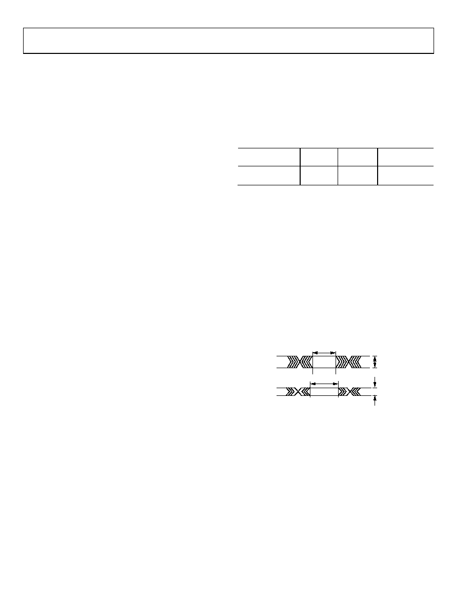
For typical silicon, decreasing the LVDS swing from 400 mV p-p
to 250 mV p-p requires the minimum data valid period to
increase by 15%. This is illustrated in Figure 100.
225ps
400mV
260ps
250mV
04862-098
Figure 100. Typical Minimum Valid Data Time (tMDE) vs. LVDS Swing
The minimum valid data window changes with temperature,
voltage, and process. The maximum value presented in the
specification table was determined from a 6σ distribution in the
worst-case conditions.
相关PDF资料 |
PDF描述 |
|---|---|
| AD7225LPZ | IC DAC 8BIT QUAD W/AMP 28-PLCC |
| AD9776BSVZ | IC DAC 12BIT DUAL 1GSPS 100TQFP |
| ADDAC80D-CBI-V | IC DAC 12BIT LOW COST 24-CDIP |
| AD7247KNZ | IC DAC 12BIT W/AMP W/BUFF 24-DIP |
| VI-2NW-IV-F1 | CONVERTER MOD DC/DC 5.5V 150W |
相关代理商/技术参数 |
参数描述 |
|---|---|
| AD9735BBCZ1 | 制造商:AD 制造商全称:Analog Devices 功能描述:10-/12-/14-Bit, 1200 MSPS DACS |
| AD9735BBCZRL | 功能描述:IC DAC 12BIT 1.2GSPS 160-CSPBGA RoHS:是 类别:集成电路 (IC) >> 数据采集 - 数模转换器 系列:- 产品培训模块:Data Converter Fundamentals DAC Architectures 标准包装:750 系列:- 设置时间:7µs 位数:16 数据接口:并联 转换器数目:1 电压电源:双 ± 功率耗散(最大):100mW 工作温度:0°C ~ 70°C 安装类型:表面贴装 封装/外壳:28-LCC(J 形引线) 供应商设备封装:28-PLCC(11.51x11.51) 包装:带卷 (TR) 输出数目和类型:1 电压,单极;1 电压,双极 采样率(每秒):143k |
| AD9735BBCZRL1 | 制造商:AD 制造商全称:Analog Devices 功能描述:10-/12-/14-Bit, 1200 MSPS DACS |
| AD9735-DPG2-EBZ | 功能描述:BOARD EVAL FOR AD9735 RoHS:是 类别:编程器,开发系统 >> 评估板 - 数模转换器 (DAC) 系列:* 产品培训模块:Lead (SnPb) Finish for COTS Obsolescence Mitigation Program 标准包装:1 系列:- DAC 的数量:4 位数:12 采样率(每秒):- 数据接口:串行,SPI? 设置时间:3µs DAC 型:电流/电压 工作温度:-40°C ~ 85°C 已供物品:板 已用 IC / 零件:MAX5581 |
| AD9735-EB | 制造商:Analog Devices 功能描述: |
发布紧急采购,3分钟左右您将得到回复。