参数资料
| 型号: | AD9735BBCZ |
| 厂商: | Analog Devices Inc |
| 文件页数: | 36/72页 |
| 文件大小: | 0K |
| 描述: | IC DAC 12BIT 1.2GSPS 160-CSPBGA |
| 产品培训模块: | Data Converter Fundamentals DAC Architectures |
| 标准包装: | 1 |
| 位数: | 12 |
| 数据接口: | 并联 |
| 转换器数目: | 1 |
| 电压电源: | 模拟和数字 |
| 功率耗散(最大): | 550mW |
| 工作温度: | -40°C ~ 85°C |
| 安装类型: | 表面贴装 |
| 封装/外壳: | 160-LFBGA,CSPBGA |
| 供应商设备封装: | 160-CSPBGA(12x12) |
| 包装: | 托盘 |
| 输出数目和类型: | 2 电流,单极 |
| 采样率(每秒): | 1.2G |
第1页第2页第3页第4页第5页第6页第7页第8页第9页第10页第11页第12页第13页第14页第15页第16页第17页第18页第19页第20页第21页第22页第23页第24页第25页第26页第27页第28页第29页第30页第31页第32页第33页第34页第35页当前第36页第37页第38页第39页第40页第41页第42页第43页第44页第45页第46页第47页第48页第49页第50页第51页第52页第53页第54页第55页第56页第57页第58页第59页第60页第61页第62页第63页第64页第65页第66页第67页第68页第69页第70页第71页第72页
AD9734/AD9735/AD9736
Rev. A | Page 41 of 72
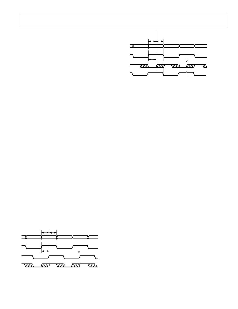
To find the leading edge of the data cycle, increment the
measured setup delay until the check bit goes low. To find the
trailing edge, increment the measured hold delay (MHD) until
check goes low. Always set MHD = 0 when incrementing MSD
and vice versa.
The incremental units of SD, MSD, and MHD are in units of real
time, not fractions of a clock cycle. The nominal step size is 80 ps.
OPERATING THE LVDS CONTROLLER IN
MANUAL MODE VIA THE SPI PORT
The manual operation of the LVDS controller allows the user to
step through both the setup and hold delays to calculate the
optimal sampling delay (that is, the center of the data eye).
With SD<3:0> and MHD<3:0> set to 0, increment the setup time
delay (MSD<3:0>, Reg. 4, Bits 7:4) until the check bit (Reg. 5,
Bit 0) goes low and record this value. This locates the leading
DATACLK_IN (and data) transition, as shown in Figure 80.
With SD<3:0> and MSD<3:0> set to 0, increment the hold time
delay (MHD<3:0>, Reg. 4, Bits 3:0) until the check bit (Reg. 5,
Bit 0) goes low and record this value. This locates the trailing
DATACLK_IN (and DB<13:0>) transition, as shown in Figure
Once both DATACLK_IN edges are located, the sample delay
(SD<3:0>, Reg. 5, Bits 7:4) must be updated by
Sample Delay = (MHD MSD)/2
After updating SD<3:0>, verify that the sampling signal is in the
middle of the valid data window by adjusting both MHD and
MSD with the new sample delay until the check bit goes low.
The new MHD and MSD values should be equal to or within
one unit delay if SD<3:0> was set correctly.
MHD and MSD may not be equal to or within one unit delay if
the external clock jitter and noise exceeds the internal delay
resolution. Differences of 2, 3, or more are possible and can
require more filtering to provide stable operation.
The sample delay calibration should be performed prior to
enabling surveillance mode or auto mode.
SETUP TIME (
tS)
SAMPLE DELAY
MSD<3:0> = 0 1 2 3 4 5
CSS SAMPLE DCS
CHECK = 1
SD<3:0>
DB<13:0>
DATACLK_IN
CSS WITH
MHD<3:0> = 0
DSC DELAYED
BY MSD<3:0>
04862-
078
Figure 80. Setup Delay Measurement
SETUP TIME (
tS)
HOLD TIME (
tH)
SAMPLE DELAY
CSS SAMPLE DCS
CHECK = 1 1 1 1 1 0
CHECK = 1
SD<3:0>
0
4862-
079
MSD<3:0> = 0 1 2 3 4 5
DB<13:0>
DATACLK_IN
CSS WITH
MHD<3:0> = 0
DSC DELAYED
BY MSD<3:0> = 0
Figure 81. Hold Delay Measurement
OPERATING THE LVDS CONTROLLER IN
SURVEILLANCE AND AUTO MODE
In surveillance mode, the controller searches for the edges of
the data eye in the same manner as in the manual mode of
operation and triggers an interrupt if the clock sampling signal
(CSS) has moved more than the threshold value set by
LTRH<1:0> (Reg. 6, Bits 1:0).
There is an internal filter that averages the setup and hold time
measurements to filter out noise and glitches on the clock lines.
Average Value = (MHD – MSD)/2
New Average = Average Value + (Δ Average/2 ^ LFLT<3:0>)
If an accumulating error in the average value causes it to exceed
the threshold value (LTHR<1:0>), an interrupt is issued.
The maximum allowable value for LFLT<3:0> is 12. If
LFLT<3:0> is too small, clock jitter and noise can cause erratic
behavior. In most cases, LFLT can be set to the maximum value.
In surveillance mode, the ideal sampling point should first be
found using manual mode and then applied to the sample delay
registers. Set the threshold and filter values depending on how
far the CSS signal is allowed to drift before an interrupt occurs.
Then, set the surveillance bit high (Reg. 6, Bit 7) and monitor
the interrupt signal either via the SPI port (Reg. 1, Bit 7) or the
IRQ pin.
In auto mode, follow the same steps to set up the sample delay,
threshold, and filter length. To run the controller in auto mode,
both the LAUTO (Reg. 6, Bit 6) and LSURV (Reg. 6, Bit 7) bits
need to be set to 1. In auto mode, the LVDS interrupt should be
set low (Reg. 1, Bit 3) to allow the sample delay to be automati-
cally updated if the threshold value is exceeded.
相关PDF资料 |
PDF描述 |
|---|---|
| AD7225LPZ | IC DAC 8BIT QUAD W/AMP 28-PLCC |
| AD9776BSVZ | IC DAC 12BIT DUAL 1GSPS 100TQFP |
| ADDAC80D-CBI-V | IC DAC 12BIT LOW COST 24-CDIP |
| AD7247KNZ | IC DAC 12BIT W/AMP W/BUFF 24-DIP |
| VI-2NW-IV-F1 | CONVERTER MOD DC/DC 5.5V 150W |
相关代理商/技术参数 |
参数描述 |
|---|---|
| AD9735BBCZ1 | 制造商:AD 制造商全称:Analog Devices 功能描述:10-/12-/14-Bit, 1200 MSPS DACS |
| AD9735BBCZRL | 功能描述:IC DAC 12BIT 1.2GSPS 160-CSPBGA RoHS:是 类别:集成电路 (IC) >> 数据采集 - 数模转换器 系列:- 产品培训模块:Data Converter Fundamentals DAC Architectures 标准包装:750 系列:- 设置时间:7µs 位数:16 数据接口:并联 转换器数目:1 电压电源:双 ± 功率耗散(最大):100mW 工作温度:0°C ~ 70°C 安装类型:表面贴装 封装/外壳:28-LCC(J 形引线) 供应商设备封装:28-PLCC(11.51x11.51) 包装:带卷 (TR) 输出数目和类型:1 电压,单极;1 电压,双极 采样率(每秒):143k |
| AD9735BBCZRL1 | 制造商:AD 制造商全称:Analog Devices 功能描述:10-/12-/14-Bit, 1200 MSPS DACS |
| AD9735-DPG2-EBZ | 功能描述:BOARD EVAL FOR AD9735 RoHS:是 类别:编程器,开发系统 >> 评估板 - 数模转换器 (DAC) 系列:* 产品培训模块:Lead (SnPb) Finish for COTS Obsolescence Mitigation Program 标准包装:1 系列:- DAC 的数量:4 位数:12 采样率(每秒):- 数据接口:串行,SPI? 设置时间:3µs DAC 型:电流/电压 工作温度:-40°C ~ 85°C 已供物品:板 已用 IC / 零件:MAX5581 |
| AD9735-EB | 制造商:Analog Devices 功能描述: |
发布紧急采购,3分钟左右您将得到回复。