参数资料
| 型号: | AD9735BBCZ |
| 厂商: | Analog Devices Inc |
| 文件页数: | 35/72页 |
| 文件大小: | 0K |
| 描述: | IC DAC 12BIT 1.2GSPS 160-CSPBGA |
| 产品培训模块: | Data Converter Fundamentals DAC Architectures |
| 标准包装: | 1 |
| 位数: | 12 |
| 数据接口: | 并联 |
| 转换器数目: | 1 |
| 电压电源: | 模拟和数字 |
| 功率耗散(最大): | 550mW |
| 工作温度: | -40°C ~ 85°C |
| 安装类型: | 表面贴装 |
| 封装/外壳: | 160-LFBGA,CSPBGA |
| 供应商设备封装: | 160-CSPBGA(12x12) |
| 包装: | 托盘 |
| 输出数目和类型: | 2 电流,单极 |
| 采样率(每秒): | 1.2G |
第1页第2页第3页第4页第5页第6页第7页第8页第9页第10页第11页第12页第13页第14页第15页第16页第17页第18页第19页第20页第21页第22页第23页第24页第25页第26页第27页第28页第29页第30页第31页第32页第33页第34页当前第35页第36页第37页第38页第39页第40页第41页第42页第43页第44页第45页第46页第47页第48页第49页第50页第51页第52页第53页第54页第55页第56页第57页第58页第59页第60页第61页第62页第63页第64页第65页第66页第67页第68页第69页第70页第71页第72页
AD9734/AD9735/AD9736
Rev. A | Page 40 of 72
The LVDS and sync controllers are independently operated in
three modes via SPI port Reg. 6 and Reg. 8:
Manual mode
Surveillance mode
Auto mode
In manual mode, all of the timing measurements and updates
are externally controlled via the SPI.
In surveillance mode, each controller takes measurements and
calculates a new optimal value continuously. The result of the
measurement is passed through an averaging filter before
evaluating the results for increased noise immunity. The filtered
result is compared to a threshold value set via Reg. 6 and Reg. 8
of the SPI port. If the error is greater than the threshold, an
interrupt is triggered and the controller stops.
Reg. 1 of the SPI port controls the interrupts with Bit 3 and Bit 2
enabling the respective interrupts and Bit 7 and Bit 6 indicating
the respective controller interrupt. If an interrupt is enabled, it
also activates the AD973x IRQ pin. To clear an interrupt, the
interrupt enable bit of the respective controller must be set to 0
for at least 1 controller clock cycle (controller clock <10 MHz).
Auto mode is almost identical to surveillance mode. Instead
of triggering an interrupt and stopping the controller, the
controller automatically updates its settings to the newly
calculated optimal value and continues to run.
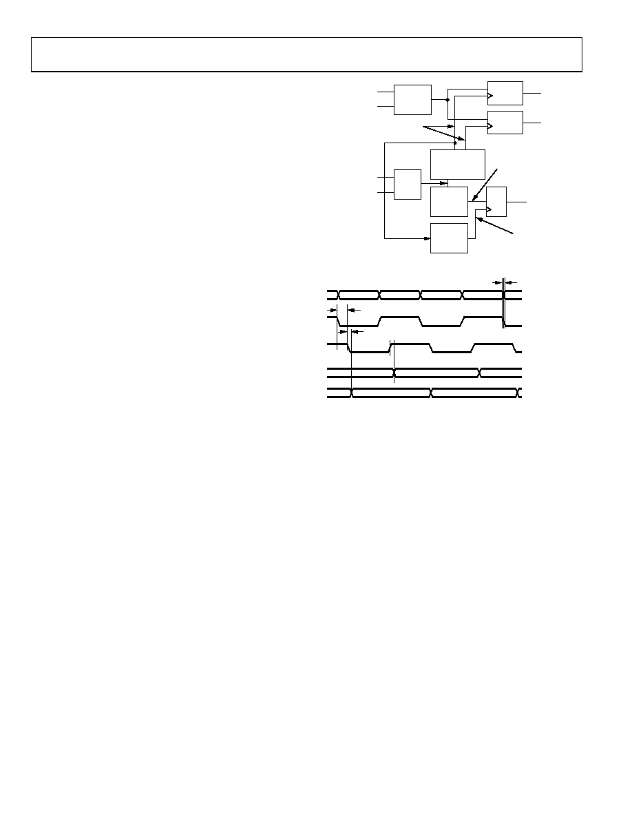
LVDS SAMPLE LOGIC
A simplified diagram of the AD973x LVDS data sampling
engine is shown in Figure 78 and the timing diagram is shown
in Figure 79.
The incoming LVDS data is latched by the data sampling signal
(DSS), which is derived from DATACLK_IN. The LVDS
controller delays DATACLK_IN to create the data sampling
signal (DSS), which is adjusted to sample the LVDS data in the
center of the valid data window. The skew between the
DATACLK_IN and the LVDS data bits (DB<13:0>) must be
minimal for proper operation. Therefore, it is recommended
that the DATACLK_IN be generated in the same manner as the
LVDS data bits (DB<13:0>) with the same driver and data lines
(that is, it should just be another LVDS data bit running a
constant 01010101… sequence, as shown in Figure 96).
If the DATACLK_IN signal is stopped, the DACCLK continues
to generate an output signal based on the last two values
clocked into the registers that drive D1 and D2, as shown in
Figure 78. If these two registers are not equal, a large output at a
frequency of one-half fDAC can be generated at the DAC output.
DB<13:0>
DATACLK_IN
LVDS
RX
DELAYED
CLOCK
SIGNAL
CLOCK
SAMPLING
SIGNAL
CHECK
D1
D2
DATA SAMPLING
SIGNAL
LVDS
RX
MSD<3:0>
DELAY
MSD<3:0>
DELAY
FF
SD<3:0>
SAMPLE DELAY
FF
DBL
DBU
04
86
2-
0
7
6
Figure 78. Internal LVDS Data Sampling Logic
SAMPLE
DELAY
PROP DELAY
TO LATCH
PROP DELAY
TO LATCH
CLK TO DB SKEW
DB13:0
D1
D2
DATACLK_IN
DATA SAMPLING
SIGNAL (DSS)
04862-
077
Figure 79. Internal LVDS Data Sampling Logic Timing
LVDS SAMPLE LOGIC CALIBRATION
The internal DSS delay must be calibrated to optimize the data
sample timing. Once calibrated, the AD973x generates an IRQ
or automatically corrects its timing if temperature or voltage
variations change the timing too much. This calibration is done
using the delayed clock sampling signal (CSS) to sample the
delayed clock signal (DCS). The LVDS sampling logic finds the
edges of the DATACLK_IN signal and, from this measurement,
the center of the valid data window is located.
The internal delay line that derives the delayed DSS from
DATACLK_IN is controlled by SD3:0 (Reg. 5, Bits 7:4), while
the DCS is controlled by MSD3:0 (Reg. 4, Bits 7:4), and the CSS
is controlled by MHD3:0 (Reg. 4, Bits 3:0).
DATACLK_IN transitions must be time aligned with the LVDS
data (DB<13:0>) transitions. This allows the CSS, derived from
the DATACLK_IN, to find the valid data window of DB<13:0>
by locating the DATACLK_IN edges. The latching (rising) edge
of CSS is initially placed using Bits SD<3:0> and can then be
shifted to the left using MSD<3:0> and to the right using
MHD<3:0>. When CSS samples the DCS and the result is 1
(which can be read back via the check bit at Reg. 5, Bit 0), the
sampling occurs in the correct data cycle.
相关PDF资料 |
PDF描述 |
|---|---|
| AD7225LPZ | IC DAC 8BIT QUAD W/AMP 28-PLCC |
| AD9776BSVZ | IC DAC 12BIT DUAL 1GSPS 100TQFP |
| ADDAC80D-CBI-V | IC DAC 12BIT LOW COST 24-CDIP |
| AD7247KNZ | IC DAC 12BIT W/AMP W/BUFF 24-DIP |
| VI-2NW-IV-F1 | CONVERTER MOD DC/DC 5.5V 150W |
相关代理商/技术参数 |
参数描述 |
|---|---|
| AD9735BBCZ1 | 制造商:AD 制造商全称:Analog Devices 功能描述:10-/12-/14-Bit, 1200 MSPS DACS |
| AD9735BBCZRL | 功能描述:IC DAC 12BIT 1.2GSPS 160-CSPBGA RoHS:是 类别:集成电路 (IC) >> 数据采集 - 数模转换器 系列:- 产品培训模块:Data Converter Fundamentals DAC Architectures 标准包装:750 系列:- 设置时间:7µs 位数:16 数据接口:并联 转换器数目:1 电压电源:双 ± 功率耗散(最大):100mW 工作温度:0°C ~ 70°C 安装类型:表面贴装 封装/外壳:28-LCC(J 形引线) 供应商设备封装:28-PLCC(11.51x11.51) 包装:带卷 (TR) 输出数目和类型:1 电压,单极;1 电压,双极 采样率(每秒):143k |
| AD9735BBCZRL1 | 制造商:AD 制造商全称:Analog Devices 功能描述:10-/12-/14-Bit, 1200 MSPS DACS |
| AD9735-DPG2-EBZ | 功能描述:BOARD EVAL FOR AD9735 RoHS:是 类别:编程器,开发系统 >> 评估板 - 数模转换器 (DAC) 系列:* 产品培训模块:Lead (SnPb) Finish for COTS Obsolescence Mitigation Program 标准包装:1 系列:- DAC 的数量:4 位数:12 采样率(每秒):- 数据接口:串行,SPI? 设置时间:3µs DAC 型:电流/电压 工作温度:-40°C ~ 85°C 已供物品:板 已用 IC / 零件:MAX5581 |
| AD9735-EB | 制造商:Analog Devices 功能描述: |
发布紧急采购,3分钟左右您将得到回复。