参数资料
| 型号: | AD9735BBCZ |
| 厂商: | Analog Devices Inc |
| 文件页数: | 4/72页 |
| 文件大小: | 0K |
| 描述: | IC DAC 12BIT 1.2GSPS 160-CSPBGA |
| 产品培训模块: | Data Converter Fundamentals DAC Architectures |
| 标准包装: | 1 |
| 位数: | 12 |
| 数据接口: | 并联 |
| 转换器数目: | 1 |
| 电压电源: | 模拟和数字 |
| 功率耗散(最大): | 550mW |
| 工作温度: | -40°C ~ 85°C |
| 安装类型: | 表面贴装 |
| 封装/外壳: | 160-LFBGA,CSPBGA |
| 供应商设备封装: | 160-CSPBGA(12x12) |
| 包装: | 托盘 |
| 输出数目和类型: | 2 电流,单极 |
| 采样率(每秒): | 1.2G |
第1页第2页第3页当前第4页第5页第6页第7页第8页第9页第10页第11页第12页第13页第14页第15页第16页第17页第18页第19页第20页第21页第22页第23页第24页第25页第26页第27页第28页第29页第30页第31页第32页第33页第34页第35页第36页第37页第38页第39页第40页第41页第42页第43页第44页第45页第46页第47页第48页第49页第50页第51页第52页第53页第54页第55页第56页第57页第58页第59页第60页第61页第62页第63页第64页第65页第66页第67页第68页第69页第70页第71页第72页
AD9734/AD9735/AD9736
Rev. A | Page 12 of 72
04862-115
A
B
C
D
E
F
DACCLK–
DACCLK+
G
H
J
K
L
M
NC
N
P
14
13
12
11
10
8
7
6
3
2
19
5
4
NC
DB8
DB9
DB10
DB11 (MSB)
DB7
DB6
DB5
DB4
DATACLK_
IN
DB3
DATACLK_
OUT
DB2
DB1
DB0
(LS
B
)
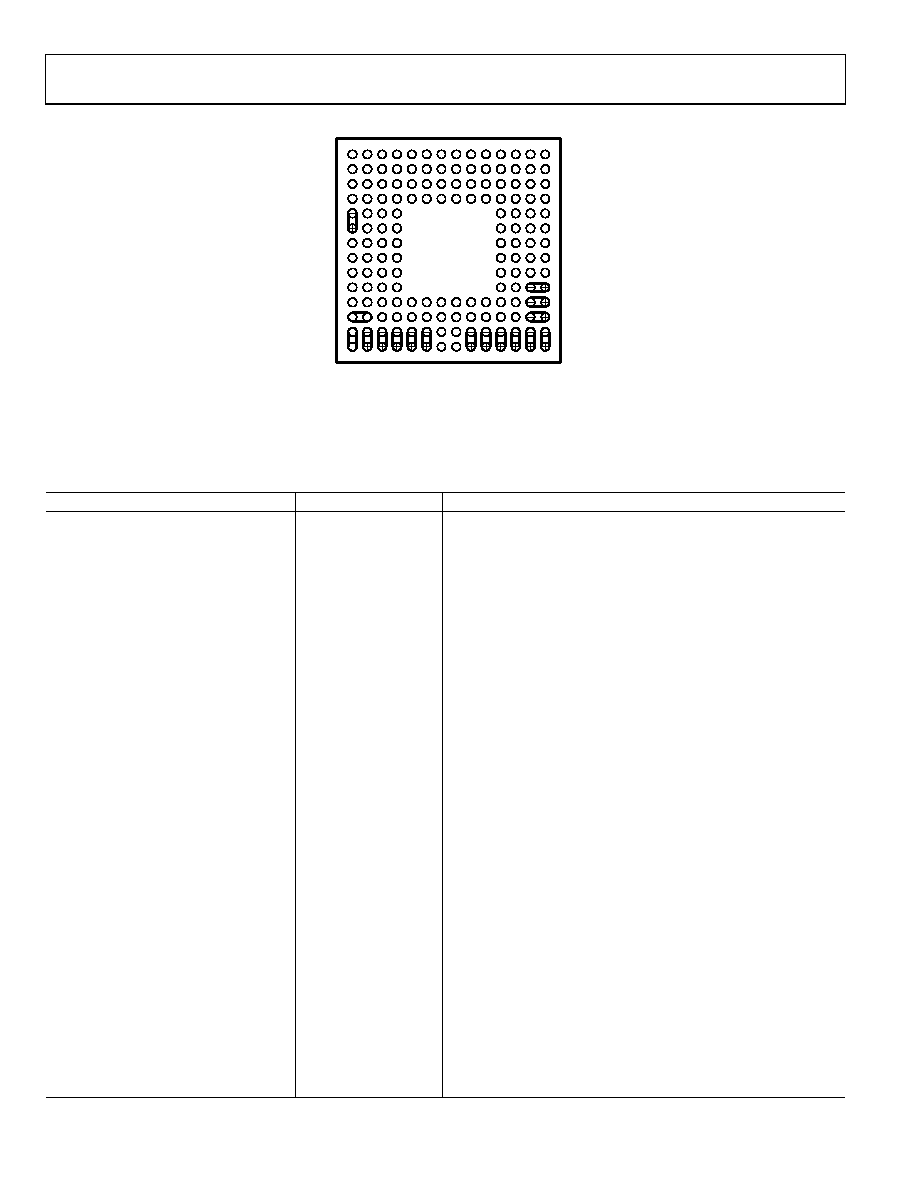
Figure 3. AD9735 Digital LVDS Input, Clock I/O (Top View)
Table 7. AD9735 Pin Function Descriptions
Pin No.
Mnemonic
Description
A1, A2, A3, B1, B2, B3, C1, C2, C3, D2, D3
CVDD18
1.8 V Clock Supply.
A4, A5, A6, A9, A10, A11, B4, B5, B6, B9,
B10, B11, C4, C5, C6, C9, C10, C11, D4, D5,
D6, D9, D10, D11
AVSS
Analog Supply Ground.
A7, B7, C7, D7
IOUTB
DAC Negative Output. 10 mA to 30 mA full-scale output current.
A8, B8, C8, D8
IOUTA
DAC Positive Output. 10 mA to 30 mA full-scale output current.
A12, A13, B12, B13, C12, C13, D12, D13
AVDD33
3.3 V Analog Supply.
A14
DNC
Do Not Connect.
B14
I120
Nominal 1.2 V Reference. Tie to analog ground via 10 kΩ resistor to
generate a 120 μA reference current.
C14
VREF
Band Gap Voltage Reference I/O. Tie to analog ground via 1 nF
capacitor; output impedance approximately 5 kΩ.
D1, E2, E3, E4, F2, F3, F4, G1, G2, G3, G4
CVSS
Clock Supply Ground.
D14
IPTAT
Factory Test Pin; Output current, proportional to absolute
temperature, is approximately 10 μA at 25°C with a slope of
approximately 20 nA/°C.
E1, F1
DACCLK/DACCLK+
Negative/Positive DAC Clock Input (DACCLK).
E11, E12, F11, F12, G11, G12
AVSS
Analog Supply Ground Shield. Tie to AVSS at the DAC.
E13
IRQ/UNSIGNED
If PIN_MODE = 0, IRQ: Active low open-drain interrupt request
output, pull up to DVDD33 with 10 kΩ resistor.
If PIN_MODE = 1, UNSIGNED: Digital input pin where 0 = twos
complement input data format, 1 = unsigned.
E14
RESET/PD
If PIN_MODE = 0, RESET: 1 resets the AD9735.
If PIN_MODE = 1, PD: 1 puts the AD9735 in the power-down state.
F13
CSB/2×
See the Serial Peripheral Interface section and the Pin Mode
Operation section for pin description.
F14
SDIO/FIFO
See the Pin Mode Operation section for pin description.
G13
SCLK/FSC0
See the Pin Mode Operation section for pin description.
G14
SDO/FSC1
See the Pin Mode Operation section for pin description.
H1, H2, H3, H4, H11, H12, H13, H14, J1, J2,
J3, J4, J11, J12, J13, J14
DVDD18
1.8 V Digital Supply.
K1, K2, K3, K4, K11, K12, L2, L3, L4, L5, L6,
L9, L10, L11, L12, M3, M4, M5, M6, M9,
M10, M11, M12
DVSS
Digital Supply Ground.
相关PDF资料 |
PDF描述 |
|---|---|
| AD7225LPZ | IC DAC 8BIT QUAD W/AMP 28-PLCC |
| AD9776BSVZ | IC DAC 12BIT DUAL 1GSPS 100TQFP |
| ADDAC80D-CBI-V | IC DAC 12BIT LOW COST 24-CDIP |
| AD7247KNZ | IC DAC 12BIT W/AMP W/BUFF 24-DIP |
| VI-2NW-IV-F1 | CONVERTER MOD DC/DC 5.5V 150W |
相关代理商/技术参数 |
参数描述 |
|---|---|
| AD9735BBCZ1 | 制造商:AD 制造商全称:Analog Devices 功能描述:10-/12-/14-Bit, 1200 MSPS DACS |
| AD9735BBCZRL | 功能描述:IC DAC 12BIT 1.2GSPS 160-CSPBGA RoHS:是 类别:集成电路 (IC) >> 数据采集 - 数模转换器 系列:- 产品培训模块:Data Converter Fundamentals DAC Architectures 标准包装:750 系列:- 设置时间:7µs 位数:16 数据接口:并联 转换器数目:1 电压电源:双 ± 功率耗散(最大):100mW 工作温度:0°C ~ 70°C 安装类型:表面贴装 封装/外壳:28-LCC(J 形引线) 供应商设备封装:28-PLCC(11.51x11.51) 包装:带卷 (TR) 输出数目和类型:1 电压,单极;1 电压,双极 采样率(每秒):143k |
| AD9735BBCZRL1 | 制造商:AD 制造商全称:Analog Devices 功能描述:10-/12-/14-Bit, 1200 MSPS DACS |
| AD9735-DPG2-EBZ | 功能描述:BOARD EVAL FOR AD9735 RoHS:是 类别:编程器,开发系统 >> 评估板 - 数模转换器 (DAC) 系列:* 产品培训模块:Lead (SnPb) Finish for COTS Obsolescence Mitigation Program 标准包装:1 系列:- DAC 的数量:4 位数:12 采样率(每秒):- 数据接口:串行,SPI? 设置时间:3µs DAC 型:电流/电压 工作温度:-40°C ~ 85°C 已供物品:板 已用 IC / 零件:MAX5581 |
| AD9735-EB | 制造商:Analog Devices 功能描述: |
发布紧急采购,3分钟左右您将得到回复。