- 您现在的位置:买卖IC网 > PDF目录20640 > ADE7753ARSZ (Analog Devices Inc)IC ENERGY METERING 1PHASE 20SSOP PDF资料下载
参数资料
| 型号: | ADE7753ARSZ |
| 厂商: | Analog Devices Inc |
| 文件页数: | 16/60页 |
| 文件大小: | 0K |
| 描述: | IC ENERGY METERING 1PHASE 20SSOP |
| 标准包装: | 66 |
| 输入阻抗: | 390 千欧 |
| 测量误差: | 0.1% |
| 电压 - 高输入/输出: | 2.4V |
| 电压 - 低输入/输出: | 0.8V |
| 电流 - 电源: | 3mA |
| 电源电压: | 4.75 V ~ 5.25 V |
| 测量仪表类型: | 单相 |
| 工作温度: | -40°C ~ 85°C |
| 安装类型: | 表面贴装 |
| 封装/外壳: | 20-SSOP(0.209",5.30mm 宽) |
| 供应商设备封装: | 20-SSOP |
| 包装: | 管件 |
| 产品目录页面: | 797 (CN2011-ZH PDF) |
| 配用: | EVAL-ADE7753ZEB-ND - BOARD EVALUATION AD7753 |
第1页第2页第3页第4页第5页第6页第7页第8页第9页第10页第11页第12页第13页第14页第15页当前第16页第17页第18页第19页第20页第21页第22页第23页第24页第25页第26页第27页第28页第29页第30页第31页第32页第33页第34页第35页第36页第37页第38页第39页第40页第41页第42页第43页第44页第45页第46页第47页第48页第49页第50页第51页第52页第53页第54页第55页第56页第57页第58页第59页第60页
�� ��
��
��ADE7753�
�THEORY� OF� OPERATION�
�ANALOG� INPUTS�
�Table� 5.� Maximum� Input� Signal� Levels� for� Channel� 1�
�The� ADE7753� has� two� fully� differential� voltage� input� channels.�
�The� maximum� differential� input� voltage� for� input� pairs� V1P/V1N�
�Max� Signal�
�Channel� 1�
�ADC� Input� Range� Selection�
�0.5� V� 0.25� V� 0.125� V�
�and� V2P/V2N� is� ±0.5� V.� In� addition,� the� maximum� signal� level�
�0.5� V�
�Gain� =� 1� ?�
�?�
�on� analog� inputs� for� V1P/V1N� and� V2P/� V2N� is� ±0.5� V� with�
�respect� to� AGND.�
�Each� analog� input� channel� has� a� programmable� gain� amplifier�
�(PGA)� with� possible� gain� selections� of� 1,� 2,� 4,� 8,� and� 16.� The�
�0.25� V�
�0.125� V�
�0.0625� V�
�0.0313� V�
�Gain� =� 2� Gain� =� 1� ?�
�Gain� =� 4� Gain� =� 2� Gain� =� 1�
�Gain� =� 8� Gain� =� 4� Gain� =� 2�
�Gain� =� 16� Gain� =� 8� Gain� =� 4�
�gain� selections� are� made� by� writing� to� the� gain� register—see�
�0.0156� V�
�?�
�Gain� =� 16� Gain� =� 8�
��0.00781� V�
�?�
�?�
�Gain� =� 16�
�and� the� gain� selection� for� the� PGA� in� Channel� 2� is� made� via�
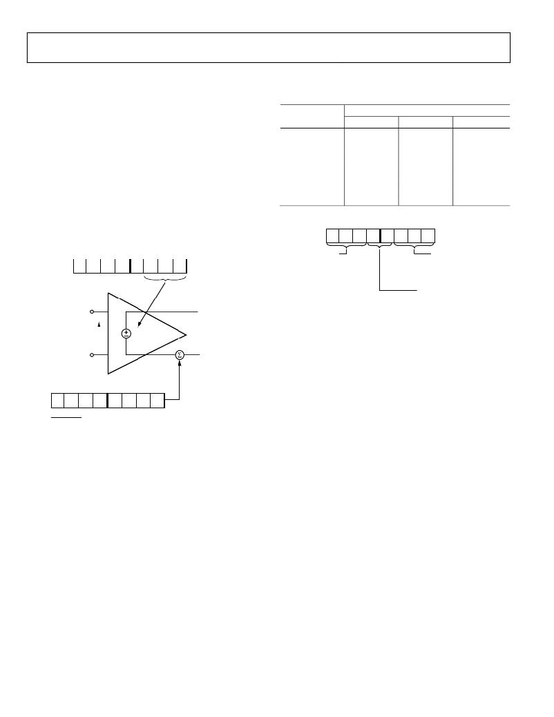
�Bits� 5� to� 7.� Figure� 31� shows� how� a� gain� selection� for� Channel� 1�
�GAIN� REGISTER*�
�CHANNEL� 1� AND� CHANNEL� 2� PGA� CONTROL�
�7� 6� 5� 4� 3� 2� 1� 0�
�is� made� using� the� gain� register.�
�0�
�0�
�0�
�0�
�0�
�0�
�0�
�0�
�ADDR:�
�0x0F�
�GAIN[7:0]�
�7�
�6�
�5�
�4� 3� 2�
�1�
�0�
�PGA� 2� GAIN� SELECT�
�000� =� � 1�
�PGA� 1� GAIN� SELECT�
�000� =� � 1�
�0�
�0�
�0�
�0�
�0�
�0�
�0�
�0�
�001� =� � 2�
�010� =� � 4�
�001� =� � 2�
�010� =� � 4�
�011� =� � 8�
�011� =� � 8�
�V1P�
�GAIN� (K)�
�SELECTION�
�100� =� � 16�
�*� REGISTER� CONTENTS�
�SHOW� POWER-ON� DEFAULTS�
�100� =� � 16�
�CHANNEL� 1� FULL-SCALE� SELECT�
�00� =� 0.5V�
�01� =� 0.25V�
�10� =� 0.125V�
�02875-0-032�
�Figure� 32.� ADE7753� Analog� Gain� Register�
�V� IN�
�V1N�
�K� � V� IN�
�+�
�OFFSET� ADJUST�
�It� is� also� possible� to� adjust� offset� errors� on� Channel� 1� and�
�Channel� 2� by� writing� to� the� offset� correction� registers,� CH1OS�
�and� CH2OS,� respectively.� These� registers� allow� channel� offsets�
�in� the� range� ±20� mV� to� ±50� mV� (depending� on� the� gain� setting)�
�to� be� removed.� Channel� 1� and� 2� offset� registers� are� sign� magni-�
�7�
�0�
�6�
�0�
�5�
�0�
�4�
�0�
�3�
�0�
�2�
�0�
�1�
�0�
�0�
�0�
�(±50mV)�
�tude� coded.� A� negative� number� is� applied� to� the� Channel� 1�
�offset� register,� CH1OS,� for� a� negative� offset� adjustment.� Note�
�CH1OS[7:0]�
�BITS� 0� to� 5:� SIGN� MAGNITUDE� CODED� OFFSET� CORRECTION�
�BIT� 6:� NOT� USED�
�BIT� 7:� DIGITAL� INTEGRATOR� (ON� =� 1,� OFF� =� 0;� DEFAULT� OFF)�
�02875-0-031�
�Figure� 31.� PGA� in� Channel� 1�
�In� addition� to� the� PGA,� Channel� 1� also� has� a� full-scale� input�
�range� selection� for� the� ADC.� The� ADC� analog� input� range�
�selection� is� also� made� using� the� gain� register—see� Figure� 32.� As�
�mentioned� previously,� the� maximum� differential� input� voltage�
�is� 0.5� V.� However,� by� using� Bits� 3� and� 4� in� the� gain� register,� the�
�maximum� ADC� input� voltage� can� be� set� to� 0.5� V,� 0.25� V,� or�
�0.125� V.� This� is� achieved� by� adjusting� the� ADC� reference—see�
�the� ADE7753� Reference� Circuit� section.� Table� 5� summarizes� the�
�maximum� differential� input� signal� level� on� Channel� 1� for� the�
�various� ADC� range� and� gain� selections.�
�that� the� Channel� 2� offset� register� is� inverted.� A� negative� number�
�is� applied� to� CH2OS� for� a� positive� offset� adjustment.� It� is� not�
�necessary� to� perform� an� offset� correction� in� an� energy� measure-�
��shows� the� effect� of� offsets� on� the� real� power� calculation.� As� seen�
�from� Figure� 33,� an� offset� on� Channel� 1� and� Channel� 2�
�contributes� a� dc� component� after� multiplication.� Because� this� dc�
�component� is� extracted� by� LPF2� to� generate� the� active� (real)�
�power� information,� the� offsets� contribute� an� error� to� the� active�
�power� calculation.� This� problem� is� easily� avoided� by� enabling�
�HPF� in� Channel� 1.� By� removing� the� offset� from� at� least� one�
�channel,� no� error� component� is� generated� at� dc� by� the�
�multiplication.� Error� terms� at� cos(� ω� t)� are� removed� by� LPF2� and�
�by� integration� of� the� active� power� signal� in� the� active� energy�
�register� (AENERGY[23:0])� —see� the� Energy� Calculation� section.�
�Rev.� C� |� Page� 16� of� 60�
�相关PDF资料 |
PDF描述 |
|---|---|
| A7SSB-1506G | CABLE D-SUB-AFM15B/AE15G/AFM15B |
| HMM06DSUS | CONN EDGECARD 12POS .156 DIP SLD |
| GCC10DCAI-S189 | CONN EDGECARD 20POS R/A .100 SLD |
| ADE7759ARSZ | IC ENERGY METERING 1PHASE 20SSOP |
| RMM40DTAD-S189 | CONN EDGECARD 80POS R/A .156 SLD |
相关代理商/技术参数 |
参数描述 |
|---|---|
| ADE7753ARSZ | 制造商:Analog Devices 功能描述:ENERGY METERING IC |
| ADE7753ARSZ | 制造商:Analog Devices 功能描述:IC MULTIFUNCTION METER |
| ADE7753ARSZRL | 功能描述:IC ENERGY METERING 1PHASE 20SSOP RoHS:是 类别:集成电路 (IC) >> PMIC - 能量测量 系列:- 产品培训模块:Lead (SnPb) Finish for COTS Obsolescence Mitigation Program 标准包装:2,500 系列:* |
| ADE7753-ARSZRL | 制造商:Analog Devices 功能描述: |
| ADE7753XRS | 制造商:Analog Devices 功能描述: |
发布紧急采购,3分钟左右您将得到回复。