- 您现在的位置:买卖IC网 > PDF目录20640 > ADE7753ARSZ (Analog Devices Inc)IC ENERGY METERING 1PHASE 20SSOP PDF资料下载
参数资料
| 型号: | ADE7753ARSZ |
| 厂商: | Analog Devices Inc |
| 文件页数: | 22/60页 |
| 文件大小: | 0K |
| 描述: | IC ENERGY METERING 1PHASE 20SSOP |
| 标准包装: | 66 |
| 输入阻抗: | 390 千欧 |
| 测量误差: | 0.1% |
| 电压 - 高输入/输出: | 2.4V |
| 电压 - 低输入/输出: | 0.8V |
| 电流 - 电源: | 3mA |
| 电源电压: | 4.75 V ~ 5.25 V |
| 测量仪表类型: | 单相 |
| 工作温度: | -40°C ~ 85°C |
| 安装类型: | 表面贴装 |
| 封装/外壳: | 20-SSOP(0.209",5.30mm 宽) |
| 供应商设备封装: | 20-SSOP |
| 包装: | 管件 |
| 产品目录页面: | 797 (CN2011-ZH PDF) |
| 配用: | EVAL-ADE7753ZEB-ND - BOARD EVALUATION AD7753 |
第1页第2页第3页第4页第5页第6页第7页第8页第9页第10页第11页第12页第13页第14页第15页第16页第17页第18页第19页第20页第21页当前第22页第23页第24页第25页第26页第27页第28页第29页第30页第31页第32页第33页第34页第35页第36页第37页第38页第39页第40页第41页第42页第43页第44页第45页第46页第47页第48页第49页第50页第51页第52页第53页第54页第55页第56页第57页第58页第59页第60页
�� �
�
�ADE7753�
�Interrupt� Timing�
�The� ADE7753� Serial� Interface� section� should� be� reviewed� first�
�before� reviewing� the� interrupt� timing.� As� previously� described,�
�when� the� IRQ� output� goes� low,� the� MCU� ISR� must� read� the�
�interrupt� status� register� to� determine� the� source� o� f th� e� interrupt.�
�When� reading� the� status� register� contents,� the� IRQ� output� is� set�
�high� on� the� last� falling� edge� of� SCLK� of� the� first� byte� transfer�
�(read� interrupt� status� register� command).� The� IRQ� output� is�
�held� high� until� the� last� bit� of� the� next� 15-bit� transfer� is� shifted�
�out� (interrupt� status� register� contents)—see� Figure� 45� .� If� an�
�interrupt� is� pending� at� this� time,� the� IRQ� output� goes� low� again.�
�If� no� interrupt� is� pending,� the� IRQ� output� stays� high.�
�TEMPERATURE� MEASUREMENT�
�The� ADE7753� also� includes� an� on-chip� temperature� sensor.� A�
�temperature� measurement� can� be� made� by� setting� Bit� 5� in� the�
�mode� register.� When� Bit� 5� is� set� logic� high� in� the� mode� register,�
�the� ADE7753� initiates� a� temperature� measurement� on� the� next�
�zero� crossing.� When� the� zero� crossing� on� Channel� 2� is� detected,�
�the� voltage� output� from� the� temperature� sensing� circuit� is�
�connected� to� ADC1� (Channel� 1)� for� digitizing.� The� resulting�
�code� is� processed� and� placed� in� the� temperature� register�
�(TEMP[7:0])� approximately� 26� μs� later� (96/CLKIN� seconds).� If�
�enabled� in� the� interrupt� enable� register� (Bit� 5),� the� IRQ� output�
�goes� active� low� when� the� temperature� conversion� is� finished.�
�The� contents� of� the� temperature� register� are� signed� (twos�
�complement)� with� a� resolution� of� approximately� 1.5� LSB/°C.�
�The� temperature� register� produces� a� code� of� 0x00� when� the�
�ambient� temperature� is� approximately� ?25°C.� The� temperature�
�measurement� is� uncalibrated� in� the� ADE7753� and� has� an� offset�
�tolerance� as� high� as� ±25°C.�
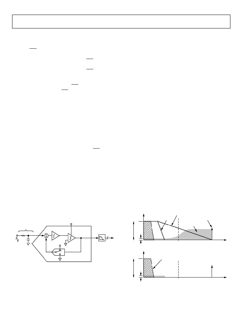
�ADE7753� ANALOG-TO-DIGITAL� CONVERSION�
�The� analog-to-digital� conversion� in� the� ADE7753� is� carried� out�
�using� two� second-order� Σ-Δ� ADCs.� For� simplicity,� the� block�
�A� Σ-Δ� modulator� converts� the� input� signal� into� a� continuous�
�serial� stream� of� 1s� and� 0s� at� a� rate� determined� by� the� sampling�
�clock.� In� the� ADE7753,� the� sampling� clock� is� equal� to� CLKIN/4.�
�The� 1-bit� DAC� in� the� feedback� loop� is� driven� by� the� serial� data�
�stream.� The� DAC� output� is� subtracted� from� the� input� signal.� If�
�the� loop� gain� is� high� enough,� the� average� value� of� the� DAC� out-�
�put� (and� therefore� the� bit� stream)� can� approach� that� of� the� input�
�signal� level.� For� any� given� input� value� in� a� single� sampling� interval,�
�the� data� from� the� 1-bit� ADC� is� virtually� meaningless.� Only� when�
�a� large� number� of� samples� are� averaged� is� a� meaningful� result�
�obtained.� This� averaging� is� carried� out� in� the� second� part� of� the�
�ADC,� the� digital� low-pass� filter.� By� averaging� a� large� number� of�
�bits� from� the� modulator,� the� low-pass� filter� can� produce� 24-bit�
�data-words� that� are� proportional� to� the� input� signal� level.�
�The� Σ-Δ� converter� uses� two� techniques� to� achieve� high� resolution�
�from� what� is� essentially� a� 1-bit� conversion� technique.� The� first�
�is� oversampling.� Oversampling� means� that� the� signal� is� sampled�
�at� a� rate� (frequency),� which� is� many� times� higher� than� the�
�bandwidth� of� interest.� For� example,� the� sampling� rate� in� the�
�ADE7753� is� CLKIN/4� (894� kHz)� and� the� band� of� interest� is�
�40� Hz� to� 2� kHz.� Oversampling� has� the� effect� of� spreading� the�
�quantization� noise� (noise� due� to� sampling)� over� a� wider�
�bandwidth.� With� the� noise� spread� more� thinly� over� a� wider�
�bandwidth,� the� quantization� noise� in� the� band� of� interest� is�
�lowered—see� Figure� 48.� However,� oversampling� alone� is� not�
�efficient� enough� to� improve� the� signal-to-noise� ratio� (SNR)� in�
�the� band� of� interest.� For� example,� an� oversampling� ratio� of� 4� is�
�required� just� to� increase� the� SNR� by� only� 6� dB� (1� bit).� To� keep�
�the� oversampling� ratio� at� a� reasonable� level,� it� is� possible� to�
�shape� the� quantization� noise� so� that� the� majority� of� the� noise�
�lies� at� the� higher� frequencies.� In� the� Σ-Δ� modulator,� the� noise� is�
�shaped� by� the� integrator,� which� has� a� high-pass-type� response�
�for� the� quantization� noise.� The� result� is� that� most� of� the� noise� is�
�at� the� higher� frequencies� where� it� can� be� removed� by� the� digital�
��diagram� in� Figure� 47� shows� a� first-order� Σ-Δ� ADC.� The� converter�
�is� made� up� of� the� Σ-Δ� modulator� and� the� digital� low-pass� filter.�
�MCLK/4�
�SIGNAL�
�DIGITAL�
�FILTER�
�ANTILALIAS�
�FILTER� (RC)�
�SHAPED�
�SAMPLING�
�FREQUENCY�
�ANALOG�
�LOW-PASS� FILTER�
�R�
�C�
�+�
�–�
�INTEGRATOR�
�+�
�–�
�LATCHED�
�COMPARATOR�
�DIGITAL�
�LOW-PASS�
�FILTER�
�24�
�NOISE�
�NOISE�
�V� REF�
�0�
�2�
�447�
�894�
�FREQUENCY� (kHz)�
�.....10100101.....�
�HIGH� RESOLUTION�
�1-BIT� DAC�
�SIGNAL�
�OUTPUT� FROM� DIGITAL�
�LPF�
�02875-0-046�
�Figure� 47.� First-Order� Σ� -?� ADC�
�NOISE�
�0�
�2�
�447�
�FREQUENCY� (kHz)�
�894�
�02875-0-047�
�Figure� 48.� Noise� Reduction� Due� to� Oversampling� and�
�Noise� Shaping� in� the� Analog� Modulator�
�Rev.� C� |� Page� 22� of� 60�
�相关PDF资料 |
PDF描述 |
|---|---|
| A7SSB-1506G | CABLE D-SUB-AFM15B/AE15G/AFM15B |
| HMM06DSUS | CONN EDGECARD 12POS .156 DIP SLD |
| GCC10DCAI-S189 | CONN EDGECARD 20POS R/A .100 SLD |
| ADE7759ARSZ | IC ENERGY METERING 1PHASE 20SSOP |
| RMM40DTAD-S189 | CONN EDGECARD 80POS R/A .156 SLD |
相关代理商/技术参数 |
参数描述 |
|---|---|
| ADE7753ARSZ | 制造商:Analog Devices 功能描述:ENERGY METERING IC |
| ADE7753ARSZ | 制造商:Analog Devices 功能描述:IC MULTIFUNCTION METER |
| ADE7753ARSZRL | 功能描述:IC ENERGY METERING 1PHASE 20SSOP RoHS:是 类别:集成电路 (IC) >> PMIC - 能量测量 系列:- 产品培训模块:Lead (SnPb) Finish for COTS Obsolescence Mitigation Program 标准包装:2,500 系列:* |
| ADE7753-ARSZRL | 制造商:Analog Devices 功能描述: |
| ADE7753XRS | 制造商:Analog Devices 功能描述: |
发布紧急采购,3分钟左右您将得到回复。