- 您现在的位置:买卖IC网 > PDF目录20640 > ADE7753ARSZ (Analog Devices Inc)IC ENERGY METERING 1PHASE 20SSOP PDF资料下载
参数资料
| 型号: | ADE7753ARSZ |
| 厂商: | Analog Devices Inc |
| 文件页数: | 23/60页 |
| 文件大小: | 0K |
| 描述: | IC ENERGY METERING 1PHASE 20SSOP |
| 标准包装: | 66 |
| 输入阻抗: | 390 千欧 |
| 测量误差: | 0.1% |
| 电压 - 高输入/输出: | 2.4V |
| 电压 - 低输入/输出: | 0.8V |
| 电流 - 电源: | 3mA |
| 电源电压: | 4.75 V ~ 5.25 V |
| 测量仪表类型: | 单相 |
| 工作温度: | -40°C ~ 85°C |
| 安装类型: | 表面贴装 |
| 封装/外壳: | 20-SSOP(0.209",5.30mm 宽) |
| 供应商设备封装: | 20-SSOP |
| 包装: | 管件 |
| 产品目录页面: | 797 (CN2011-ZH PDF) |
| 配用: | EVAL-ADE7753ZEB-ND - BOARD EVALUATION AD7753 |
第1页第2页第3页第4页第5页第6页第7页第8页第9页第10页第11页第12页第13页第14页第15页第16页第17页第18页第19页第20页第21页第22页当前第23页第24页第25页第26页第27页第28页第29页第30页第31页第32页第33页第34页第35页第36页第37页第38页第39页第40页第41页第42页第43页第44页第45页第46页第47页第48页第49页第50页第51页第52页第53页第54页第55页第56页第57页第58页第59页第60页
�� �
�
�ADE7753�
�Antialias� Filter�
��to� the� modulator.� This� filter� is� present� to� prevent� aliasing.�
�Aliasing� is� an� artifact� of� all� sampled� systems.� Aliasing� means�
�that� frequency� components� in� the� input� signal� to� the� ADC,�
�which� are� higher� than� half� the� sampling� rate� of� the� ADC,�
�appear� in� the� sampled� signal� at� a� frequency� below� half� the�
�sampling� rate.� Figure� 49� illustrates� the� effect.� Frequency�
�components� (arrows� shown� in� black)� above� half� the� sampling�
�frequency� (also� know� as� the� Nyquist� frequency,� i.e.,� 447� kHz)�
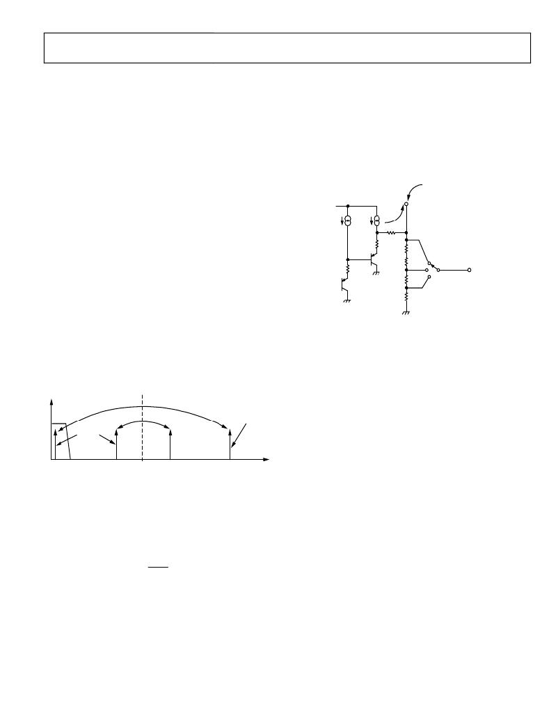
�ADE7753� Reference� Circuit�
��circuitry.� The� nominal� reference� voltage� at� the� REF� IN/OUT� pin� is�
�2.42� V.� This� is� the� reference� voltage� used� for� the� ADCs� in� the�
�ADE7753.� However,� Channel� 1� has� three� input� range� selections�
�that� are� selected� by� dividing� down� the� reference� value� used� for�
�the� ADC� in� Channel� 1.� The� reference� value� used� for� Channel� 1�
�is� divided� down� to� ?� and� ?� of� the� nominal� value� by� using� an�
��OUTPUT�
�are� imaged� or� folded� back� down� below� 447� kHz.� This� happens�
�with� all� ADCs� regardless� of� the� architecture.� In� the� example�
�MAXIMUM�
�LOAD� =� 10� μ� A�
�IMPEDANCE�
�6k� Ω�
�REF� IN/OUT�
�shown,� only� frequencies� near� the� sampling� frequency,� i.e.,�
�894� kHz,� move� into� the� band� of� interest� for� metering,� i.e.,� 40� Hz�
�PTAT�
�60� μ� A�
�1.7k� Ω�
�2.42V�
�to� 2� kHz.� This� allows� the� use� of� a� very� simple� LPF� (low-pass�
�filter)� to� attenuate� high� frequency� (near� 900� kHz)� noise,� and�
�prevents� distortion� in� the� band� of� interest.� For� conventional�
�current� sensors,� a� simple� RC� filter� (single-pole� LPF)� with� a�
�2.5V�
�12.5k� Ω�
�12.5k� Ω�
�corner� frequency� of� 10� kHz� produces� an� attenuation� of�
�approximately� 40� dB� at� 894� kHz—see� Figure� 49.� The� 20� dB� per�
�decade� attenuation� is� usually� sufficient� to� eliminate� the� effects�
�12.5k� Ω�
�12.5k� Ω�
�REFERENCE� INPUT�
�TO� ADC� CHANNEL� 1�
�(RANGE� SELECT)�
�2.42V,� 1.21V,� 0.6V�
�of� aliasing� for� conventional� current� sensors.� However,� for� a�
�di/dt� sensor� such� as� a� Rogowski� coil,� the� sensor� has� a� 20� dB� per�
�decade� gain.� This� neutralizes� the� –20� dB� per� decade� attenuation�
�produced� by� one� simple� LPF.� Therefore,� when� using� a� di/dt�
�sensor,� care� should� be� taken� to� offset� the� 20� dB� per� decade� gain.�
�One� simple� approach� is� to� cascade� two� RC� filters� to� produce� the�
�–40� dB� per� decade� attenuation� needed.�
�ALIASING� EFFECTS�
�02875-0-049�
�Figure� 50.� ADE7753� Reference� Circuit� Output�
�The� REF� IN/OUT� pin� can� be� overdriven� by� an� external� source,� for�
�example,� an� external� 2.5� V� reference.� Note� that� the� nominal�
�reference� value� supplied� to� the� ADCs� is� now� 2.5� V,� not� 2.42� V,�
�which� has� the� effect� of� increasing� the� nominal� analog� input�
�signal� range� by� 2.5/2.42� � 100%� =� 3%� or� from� 0.5� V� to� 0.5165� V.�
�The� voltage� of� the� ADE7753� reference� drifts� slightly� with�
�IMAGE�
�FREQUENCIES�
�SAMPLING�
�FREQUENCY�
�temperature—see� the� ADE7753� Specifications� for� the� temperature�
�coefficient� specification� (in� ppm/°C).� The� value� of� the� temperature�
�drift� varies� from� part� to� part.� Since� the� reference� is� used� for� the�
�ADCs� in� both� Channels� 1� and� 2,� any� x%� drift� in� the� reference�
�results� in� 2×%� deviation� of� the� meter� accuracy.� The� reference�
�0�
�2�
�447�
�FREQUENCY� (kHz)�
�894�
�02875-0-048�
�drift� resulting� from� temperature� changes� is� usually� very� small�
�and� it� is� typically� much� smaller� than� the� drift� of� other� components�
�Figure� 49.� ADC� and� Signal� Processing� in� Channel� 1� Outline� Dimensions�
�ADC� Transfer� Function�
�The� following� expression� relates� the� output� of� the� LPF� in� the�
�Σ-Δ� ADC� to� the� analog� input� signal� level.� Both� ADCs� in� the�
�ADE7753� are� designed� to� produce� the� same� output� code� for� the�
�same� input� signal� level.�
�on� a� meter.� However,� if� guaranteed� temperature� performance�
�is� needed,� one� needs� to� use� an� external� voltage� reference.�
�Alternatively,� the� meter� can� be� calibrated� at� multiple� temperatures.�
�Real-time� compensation� can� be� achieved� easily� by� using� the�
�on-chip� temperature� sensor.�
�CHANNEL� 1� ADC�
�Code� (� ADC� )� =� 3� .� 0492� �
�V� IN�
�V� OUT�
�� 262� ,� 144�
�(1)�
��Channel� 1.� In� waveform� sampling� mode,� the� ADC� outputs� a�
�signed� twos� complement� 24-bit� data-word� at� a� maximum� of�
�Therefore� with� a� full-scale� signal� on� the� input� of� 0.5� V� and� an�
�internal� reference� of� 2.42� V,� the� ADC� output� code� is� nominally�
�165,151� or� 2851Fh.� The� maximum� code� from� the� ADC� is�
�±262,144;� this� is� equivalent� to� an� input� signal� level� of� ±0.794� V.�
�However,� for� specified� performance,� it� is� recommended� that� the�
�27.9� kSPS� (CLKIN/128).� With� the� specified� full-scale� analog�
�input� signal� of� 0.5� V� (or� 0.25� V� or� 0.125� V—see� the� Analog�
�Inputs� section)� the� ADC� produces� an� output� code� that� is�
�approximately� between� 0x2851EC� (+2,642,412d)� and�
��full-scale� input� signal� level� of� 0.5� V� not� be� exceeded.�
�Rev.� C� |� Page� 23� of� 60�
�相关PDF资料 |
PDF描述 |
|---|---|
| A7SSB-1506G | CABLE D-SUB-AFM15B/AE15G/AFM15B |
| HMM06DSUS | CONN EDGECARD 12POS .156 DIP SLD |
| GCC10DCAI-S189 | CONN EDGECARD 20POS R/A .100 SLD |
| ADE7759ARSZ | IC ENERGY METERING 1PHASE 20SSOP |
| RMM40DTAD-S189 | CONN EDGECARD 80POS R/A .156 SLD |
相关代理商/技术参数 |
参数描述 |
|---|---|
| ADE7753ARSZ | 制造商:Analog Devices 功能描述:ENERGY METERING IC |
| ADE7753ARSZ | 制造商:Analog Devices 功能描述:IC MULTIFUNCTION METER |
| ADE7753ARSZRL | 功能描述:IC ENERGY METERING 1PHASE 20SSOP RoHS:是 类别:集成电路 (IC) >> PMIC - 能量测量 系列:- 产品培训模块:Lead (SnPb) Finish for COTS Obsolescence Mitigation Program 标准包装:2,500 系列:* |
| ADE7753-ARSZRL | 制造商:Analog Devices 功能描述: |
| ADE7753XRS | 制造商:Analog Devices 功能描述: |
发布紧急采购,3分钟左右您将得到回复。