- 您现在的位置:买卖IC网 > PDF目录19403 > ADSP-BF504KCPZ-4F (Analog Devices Inc)IC CCD SIGNAL PROCESSOR 88LFCSP PDF资料下载
参数资料
| 型号: | ADSP-BF504KCPZ-4F |
| 厂商: | Analog Devices Inc |
| 文件页数: | 60/80页 |
| 文件大小: | 0K |
| 描述: | IC CCD SIGNAL PROCESSOR 88LFCSP |
| 视频文件: | Blackfin? BF50x Processor Family |
| 标准包装: | 1 |
| 系列: | Blackfin® |
| 类型: | 定点 |
| 接口: | CAN,EBI/EMI,I²C,IrDA,PPI,SPI,SPORT,UART/USART |
| 时钟速率: | 400MHz |
| 非易失内存: | 闪存(16MB) |
| 芯片上RAM: | 68kB |
| 电压 - 输入/输出: | 3.30V |
| 电压 - 核心: | 1.31V |
| 工作温度: | 0°C ~ 70°C |
| 安装类型: | 表面贴装 |
| 封装/外壳: | 88-VFQFN 裸露焊盘,CSP |
| 供应商设备封装: | 88-LFCSP(12x12) |
| 包装: | 托盘 |
第1页第2页第3页第4页第5页第6页第7页第8页第9页第10页第11页第12页第13页第14页第15页第16页第17页第18页第19页第20页第21页第22页第23页第24页第25页第26页第27页第28页第29页第30页第31页第32页第33页第34页第35页第36页第37页第38页第39页第40页第41页第42页第43页第44页第45页第46页第47页第48页第49页第50页第51页第52页第53页第54页第55页第56页第57页第58页第59页当前第60页第61页第62页第63页第64页第65页第66页第67页第68页第69页第70页第71页第72页第73页第74页第75页第76页第77页第78页第79页第80页
Rev. A
|
Page 63 of 80
|
July 2011
ADSP-BF504/ADSP-BF504F/ADSP-BF506F
Analog Inputs
The ADC has a total of 12 analog inputs. Each on-board ADC
has six analog inputs that can be configured as six single-ended
channels, three pseudo differential channels, or three fully dif-
ferential channels. These may be selected as described in the
Analog Input Selection section.
Single-Ended Mode
The ADC can have a total of 12 single-ended analog input chan-
nels. In applications where the signal source has high
impedance, it is recommended to buffer the analog input
before applying it to the ADC. The analog input range can be
programmed to be either 0 to VREF or 0 to 2 × VREF.
If the analog input signal to be sampled is bipolar, the internal
reference of the ADC can be used to externally bias up this sig-
nal to make it correctly formatted for the ADC. Figure 68 shows
a typical connection diagram when operating the ADC in sin-
gle-ended mode.
Differential Mode
The ADC can have a total of six differential analog input pairs.
Differential signals have some benefits over single-ended sig-
nals, including noise immunity based on the device’s common-
mode rejection and improvements in distortion performance.
Figure 69 (Differential Input Definition) defines the fully differ-
ential analog input of the ADC.
The amplitude of the differential signal is the difference between
the signals applied to the VIN+ and VIN– pins in each differential
pair (VIN+ VIN–). VIN+ and VIN– should be simultaneously driven
by two signals each of amplitude VREF (or 2 × VREF, depending
on the range chosen) that are 180° out of phase. The amplitude
of the differential signal is, therefore (assuming the 0 to VREF
range is selected) –VREF to +VREF peak-to-peak (2 × VREF),
regardless of the common mode (CM).
The common mode is the average of the two signals
(VIN+ + VIN–)/2
and is, therefore, the voltage on which the two inputs are
centered.
This results in the span of each input being CM ± VREF/2. This
voltage has to be set up externally and its range varies with the
reference value, VREF. As the value of VREF increases, the com-
mon-mode range decreases. When driving the inputs with an
amplifier, the actual common-mode range is determined by the
amplifier’s output voltage swing.
Range vs. VREF (2 × VREF Range, VDD = 5 V)) show how the
common-mode range typically varies with VREF for a 5 V power
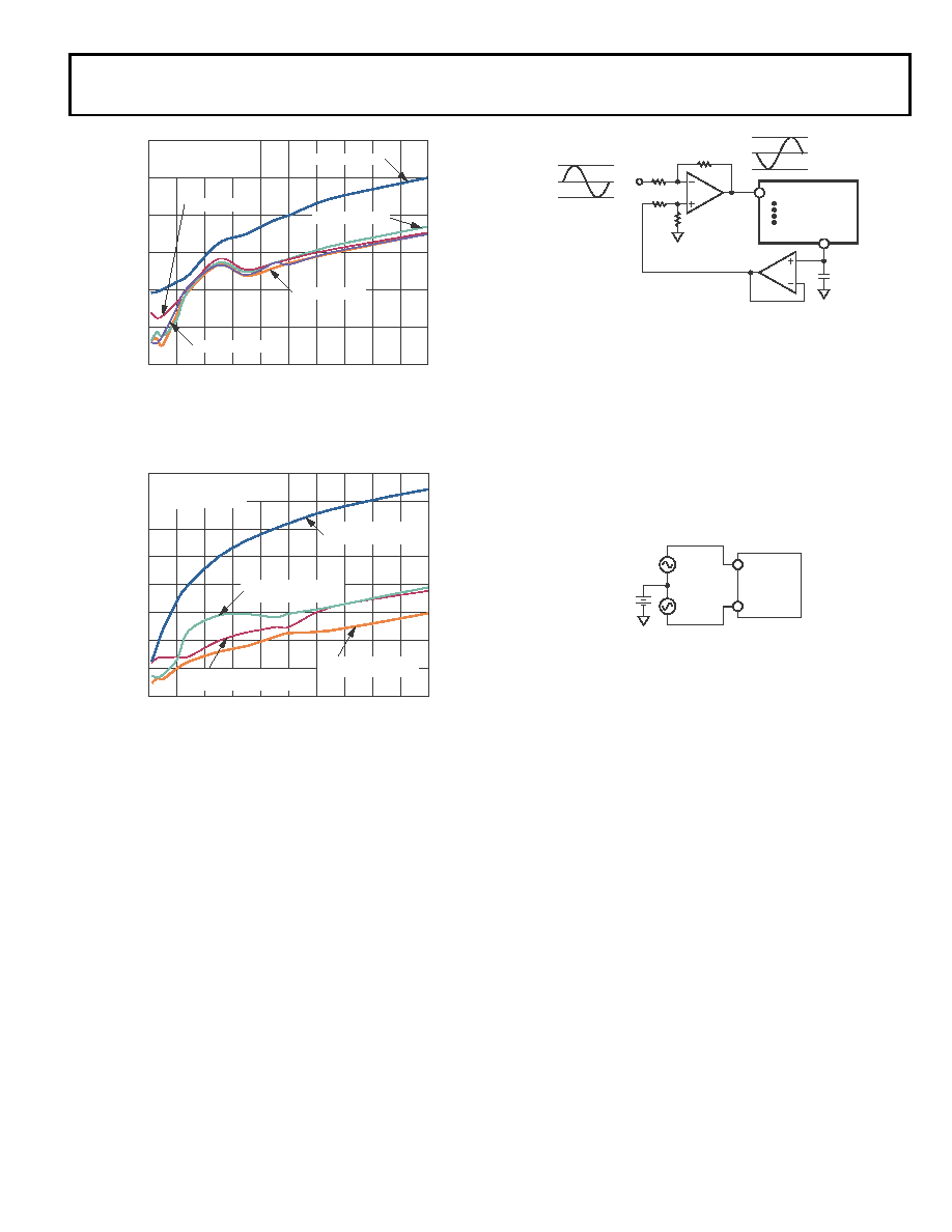
Figure 66. THD vs. Analog Input Frequency for
Various Source Impedances, Differential Mode
Figure 67. THD vs. Analog Input Frequency for Various Supply Voltages
INPUT FREQUENCY (kHz)
600
700
800
900 1000
0
200
100
400
300
500
THD
(dB)
–60
–65
–70
–75
–80
–85
–90
FSAMPLE = 1.5MSPS
VDD = 3V
RANGE = 0V TO VREF
RSOURCE = 300
RSOURCE = 0
RSOURCE = 10
RSOURCE = 47
RSOURCE = 100
INPUT FREQUENCY (kHz)
600
700
800
900 1000
0
200
100
400
300
500
THD
(dB)
–50
–60
–55
–65
–70
–75
–80
–85
–90
VDD = 3V
SINGLE-ENDED MODE
VDD = 5V
SINGLE-ENDED MODE
VDD = 3V
DIFFERENTIAL MODE
VDD = 5V
DIFFERENTIAL MODE
FSAMPLE = 1.5MSPS/2MSPS
VDD = 3V/5V
RANGE = 0 TO VREF
Figure 68. Single-Ended Mode Connection Diagram
Figure 69. Differential Input Definition
VIN
0V
+1.25V
–1.25V
V
REF
(DCAPA/DCAPB)
VA1
ADC
1
VB6
R
3R
R
0V
+2.5V
0.47μF
1ADDITIONAL PINS OMITTED FOR CLARITY.
VIN+
ADC
1
VIN–
VREF p-p
COMMON
MODE
VOLTAGE
1ADDITIONAL PINS OMITTED FOR CLARITY.
相关PDF资料 |
PDF描述 |
|---|---|
| TPSB476K010H0500 | CAP TANT 47UF 10V 10% 1210 |
| GBC08DREN | CONN EDGECARD 16POS .100 EYELET |
| CS48540-DQZR | IC DSP HP 32BIT 8CH I/O 48-QFP |
| 2300HT-220-V-RC | INDUCTOR TOROID 22UH 15% VERT |
| JWT75-5FF/A | PS TRIPLE OUTPUT +5V/+15V/-15V |
相关代理商/技术参数 |
参数描述 |
|---|---|
| ADSP-BF506BSWZ-3F | 功能描述:IC DSP 400MHZ 1.4V 120LQFP RoHS:是 类别:集成电路 (IC) >> 嵌入式 - DSP(数字式信号处理器) 系列:Blackfin® 标准包装:40 系列:TMS320DM64x, DaVinci™ 类型:定点 接口:I²C,McASP,McBSP 时钟速率:400MHz 非易失内存:外部 芯片上RAM:160kB 电压 - 输入/输出:3.30V 电压 - 核心:1.20V 工作温度:0°C ~ 90°C 安装类型:表面贴装 封装/外壳:548-BBGA,FCBGA 供应商设备封装:548-FCBGA(27x27) 包装:托盘 配用:TMDSDMK642-0E-ND - DEVELPER KIT W/NTSC CAMERA296-23038-ND - DSP STARTER KIT FOR TMS320C6416296-23059-ND - FLASHBURN PORTING KIT296-23058-ND - EVAL MODULE FOR DM642TMDSDMK642-ND - DEVELOPER KIT W/NTSC CAMERA |
| ADSP-BF506BSWZ-4F | 功能描述:IC DSP 400MHZ 1.4V 120LQFP RoHS:是 类别:集成电路 (IC) >> 嵌入式 - DSP(数字式信号处理器) 系列:Blackfin® 标准包装:40 系列:TMS320DM64x, DaVinci™ 类型:定点 接口:I²C,McASP,McBSP 时钟速率:400MHz 非易失内存:外部 芯片上RAM:160kB 电压 - 输入/输出:3.30V 电压 - 核心:1.20V 工作温度:0°C ~ 90°C 安装类型:表面贴装 封装/外壳:548-BBGA,FCBGA 供应商设备封装:548-FCBGA(27x27) 包装:托盘 配用:TMDSDMK642-0E-ND - DEVELPER KIT W/NTSC CAMERA296-23038-ND - DSP STARTER KIT FOR TMS320C6416296-23059-ND - FLASHBURN PORTING KIT296-23058-ND - EVAL MODULE FOR DM642TMDSDMK642-ND - DEVELOPER KIT W/NTSC CAMERA |
| ADSP-BF506BSWZ-4FX | 制造商:Analog Devices 功能描述:- Trays |
| ADSP-BF506F | 制造商:Analog Devices 功能描述:LOW POWER BLACKFIN WITH ADVANCED EMBEDDED CONNECTIVITY - Bulk |
| ADSPBF506FBSWZ-ENG | 制造商:Analog Devices 功能描述:- Trays |
发布紧急采购,3分钟左右您将得到回复。