- 您现在的位置:买卖IC网 > PDF目录19403 > ADSP-BF504KCPZ-4F (Analog Devices Inc)IC CCD SIGNAL PROCESSOR 88LFCSP PDF资料下载
参数资料
| 型号: | ADSP-BF504KCPZ-4F |
| 厂商: | Analog Devices Inc |
| 文件页数: | 63/80页 |
| 文件大小: | 0K |
| 描述: | IC CCD SIGNAL PROCESSOR 88LFCSP |
| 视频文件: | Blackfin? BF50x Processor Family |
| 标准包装: | 1 |
| 系列: | Blackfin® |
| 类型: | 定点 |
| 接口: | CAN,EBI/EMI,I²C,IrDA,PPI,SPI,SPORT,UART/USART |
| 时钟速率: | 400MHz |
| 非易失内存: | 闪存(16MB) |
| 芯片上RAM: | 68kB |
| 电压 - 输入/输出: | 3.30V |
| 电压 - 核心: | 1.31V |
| 工作温度: | 0°C ~ 70°C |
| 安装类型: | 表面贴装 |
| 封装/外壳: | 88-VFQFN 裸露焊盘,CSP |
| 供应商设备封装: | 88-LFCSP(12x12) |
| 包装: | 托盘 |
第1页第2页第3页第4页第5页第6页第7页第8页第9页第10页第11页第12页第13页第14页第15页第16页第17页第18页第19页第20页第21页第22页第23页第24页第25页第26页第27页第28页第29页第30页第31页第32页第33页第34页第35页第36页第37页第38页第39页第40页第41页第42页第43页第44页第45页第46页第47页第48页第49页第50页第51页第52页第53页第54页第55页第56页第57页第58页第59页第60页第61页第62页当前第63页第64页第65页第66页第67页第68页第69页第70页第71页第72页第73页第74页第75页第76页第77页第78页第79页第80页
Rev. A
|
Page 66 of 80
|
July 2011
ADSP-BF504/ADSP-BF504F/ADSP-BF506F
required acquisition time for the next sampling instant at Point
B; therefore, the analog inputs are configured as differential for
that conversion.
The channels used for simultaneous conversions are selected via
the multiplexer address input pins, A0 to A2. The logic states of
these pins also need to be established prior to the acquisition
time; however, they may change during the conversion time
provided the mode is not changed. If the mode is changed from
fully differential to pseudo differential, for example, then the
acquisition time would start again from this point. The selected
input channels are decoded as shown in Table 53 (Analog Input
The analog input range of the ADC can be selected as 0 V to
VREF or 0 V to 2 × VREF via the RANGE pin. This selection is
made in a similar fashion to that of the SGL/DIFF pin by setting
the logic state of the RANGE pin a time tacq prior to the falling
edge of CS. Subsequent to this, the logic level on this pin can be
altered after the third falling edge of ADSCLK. If this pin is tied
to a logic low, the analog input range selected is 0 V to VREF. If
this pin is tied to a logic high, the analog input range selected is
0 V to 2 × VREF.
Output Coding
The ADC output coding is set to either twos complement or
straight binary, depending on which analog input configuration
is selected for a conversion. Table 52 (ADC Output Coding)
shows which output coding scheme is used for each possible
analog input configuration.
Transfer Functions
The designed code transitions occur at successive integer LSB
values (1 LSB, 2 LSB, and so on). In single-ended mode, the LSB
size is VREF/4096 when the 0 V to VREF range is used, and the LSB
size is 2 × VREF/4096 when the 0 V to 2 × VREF range is used. In
differential mode, the LSB size is 2 × VREF /4096 when the 0 V to
VREF range is used, and the LSB size is 4 × VREF/4096 when the 0
V to 2 × VREF range is used. The ideal transfer characteristic for
the ADC when straight binary coding is output is shown in
ideal transfer characteristic for the ADC when twos comple-
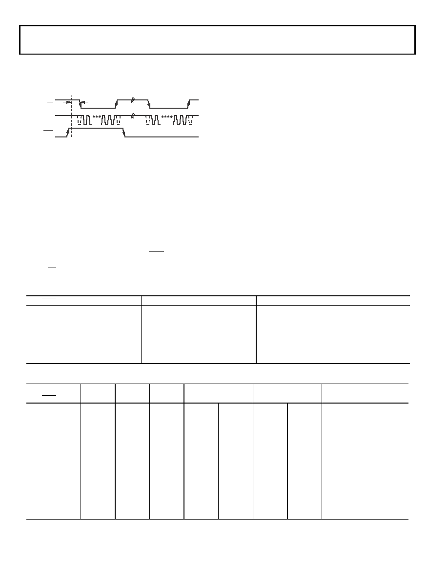
Figure 77. Selecting Differential or Single-Ended Configuration
ADSCLK
CS
114
14
1
A
SGL/DIFF
B
tACQ
Table 52. ADC Output Coding
SGL/DIFF
RANGE
Output Coding
0
(Differential Input)
0
(0 V to VREF)
Twos complement
0
(Differential Input)
1
(0 V to 2 × VREF)
Twos complement
1
(Single-Ended Input)
0
(0 V to VREF)
Straight binary
1
(Single-Ended Input)
1
(0 V to2 × VREF)
Twos complement
0
(Pseudo-Differential Input)
0
(0 V to VREF)
Straight binary
0
(Pseudo-Differential Input)
1
(0 V to 2 × VREF)
Twos complement
Table 53. Analog Input Type and Channel Selection
ADC A
ADC B
SGL/DIFF
A2
A1
A0
VIN+
VIN–
VIN+
VIN–
Comment
10
0
VA1
AGND
VB1
AGND
Single ended
10
0
1
VA2
AGND
VB2
AGND
Single ended
10
1
0
VA3
AGND
VB3
AGND
Single ended
10
1
VA4
AGND
VB4
AGND
Single ended
11
0
VA5
AGND
VB5
AGND
Single ended
11
0
1
VA6
AGND
VB6
AGND
Single ended
00
0
VA1
VA2
VB1
VB2
Fully differential
00
0
1
VA1
VA2
VB1
VB2
Pseudo differential
00
1
0
VA3
VA4
VB3
VB4
Fully differential
00
1
VA3
VA4
VB3
VB4
Pseudo differential
01
0
VA5
VA6
VB5
VB6
Fully differential
01
0
1
VA5
VA6
VB5
VB6
Pseudo differential
相关PDF资料 |
PDF描述 |
|---|---|
| TPSB476K010H0500 | CAP TANT 47UF 10V 10% 1210 |
| GBC08DREN | CONN EDGECARD 16POS .100 EYELET |
| CS48540-DQZR | IC DSP HP 32BIT 8CH I/O 48-QFP |
| 2300HT-220-V-RC | INDUCTOR TOROID 22UH 15% VERT |
| JWT75-5FF/A | PS TRIPLE OUTPUT +5V/+15V/-15V |
相关代理商/技术参数 |
参数描述 |
|---|---|
| ADSP-BF506BSWZ-3F | 功能描述:IC DSP 400MHZ 1.4V 120LQFP RoHS:是 类别:集成电路 (IC) >> 嵌入式 - DSP(数字式信号处理器) 系列:Blackfin® 标准包装:40 系列:TMS320DM64x, DaVinci™ 类型:定点 接口:I²C,McASP,McBSP 时钟速率:400MHz 非易失内存:外部 芯片上RAM:160kB 电压 - 输入/输出:3.30V 电压 - 核心:1.20V 工作温度:0°C ~ 90°C 安装类型:表面贴装 封装/外壳:548-BBGA,FCBGA 供应商设备封装:548-FCBGA(27x27) 包装:托盘 配用:TMDSDMK642-0E-ND - DEVELPER KIT W/NTSC CAMERA296-23038-ND - DSP STARTER KIT FOR TMS320C6416296-23059-ND - FLASHBURN PORTING KIT296-23058-ND - EVAL MODULE FOR DM642TMDSDMK642-ND - DEVELOPER KIT W/NTSC CAMERA |
| ADSP-BF506BSWZ-4F | 功能描述:IC DSP 400MHZ 1.4V 120LQFP RoHS:是 类别:集成电路 (IC) >> 嵌入式 - DSP(数字式信号处理器) 系列:Blackfin® 标准包装:40 系列:TMS320DM64x, DaVinci™ 类型:定点 接口:I²C,McASP,McBSP 时钟速率:400MHz 非易失内存:外部 芯片上RAM:160kB 电压 - 输入/输出:3.30V 电压 - 核心:1.20V 工作温度:0°C ~ 90°C 安装类型:表面贴装 封装/外壳:548-BBGA,FCBGA 供应商设备封装:548-FCBGA(27x27) 包装:托盘 配用:TMDSDMK642-0E-ND - DEVELPER KIT W/NTSC CAMERA296-23038-ND - DSP STARTER KIT FOR TMS320C6416296-23059-ND - FLASHBURN PORTING KIT296-23058-ND - EVAL MODULE FOR DM642TMDSDMK642-ND - DEVELOPER KIT W/NTSC CAMERA |
| ADSP-BF506BSWZ-4FX | 制造商:Analog Devices 功能描述:- Trays |
| ADSP-BF506F | 制造商:Analog Devices 功能描述:LOW POWER BLACKFIN WITH ADVANCED EMBEDDED CONNECTIVITY - Bulk |
| ADSPBF506FBSWZ-ENG | 制造商:Analog Devices 功能描述:- Trays |
发布紧急采购,3分钟左右您将得到回复。