- 您现在的位置:买卖IC网 > PDF目录19403 > ADSP-BF504KCPZ-4F (Analog Devices Inc)IC CCD SIGNAL PROCESSOR 88LFCSP PDF资料下载
参数资料
| 型号: | ADSP-BF504KCPZ-4F |
| 厂商: | Analog Devices Inc |
| 文件页数: | 64/80页 |
| 文件大小: | 0K |
| 描述: | IC CCD SIGNAL PROCESSOR 88LFCSP |
| 视频文件: | Blackfin? BF50x Processor Family |
| 标准包装: | 1 |
| 系列: | Blackfin® |
| 类型: | 定点 |
| 接口: | CAN,EBI/EMI,I²C,IrDA,PPI,SPI,SPORT,UART/USART |
| 时钟速率: | 400MHz |
| 非易失内存: | 闪存(16MB) |
| 芯片上RAM: | 68kB |
| 电压 - 输入/输出: | 3.30V |
| 电压 - 核心: | 1.31V |
| 工作温度: | 0°C ~ 70°C |
| 安装类型: | 表面贴装 |
| 封装/外壳: | 88-VFQFN 裸露焊盘,CSP |
| 供应商设备封装: | 88-LFCSP(12x12) |
| 包装: | 托盘 |
第1页第2页第3页第4页第5页第6页第7页第8页第9页第10页第11页第12页第13页第14页第15页第16页第17页第18页第19页第20页第21页第22页第23页第24页第25页第26页第27页第28页第29页第30页第31页第32页第33页第34页第35页第36页第37页第38页第39页第40页第41页第42页第43页第44页第45页第46页第47页第48页第49页第50页第51页第52页第53页第54页第55页第56页第57页第58页第59页第60页第61页第62页第63页当前第64页第65页第66页第67页第68页第69页第70页第71页第72页第73页第74页第75页第76页第77页第78页第79页第80页
Rev. A
|
Page 67 of 80
|
July 2011
ADSP-BF504/ADSP-BF504F/ADSP-BF506F
Serial Interface Voltage Drive
The ADC also has a VDRIVE feature to control the voltage at
which the serial interface operates. VDRIVE allows the ADC to
easily interface to both 3 V and 5 V processors. For example, if
the ADC was operated with a AVDD/DVDD of 5 V, the VDRIVE pin
could be powered from a 3 V supply, best ADC performance
low voltage digital processors. Therefore, the ADC could be
used with the 2 × VREF input range, with a AVDD/DVDD of 5 V
while still being able to serial interface to 3 V digital I/O parts.
ADC—MODES OF OPERATION
The mode of operation of the ADC is selected by controlling the
(logic) state of the CS signal during a conversion. There are
three possible modes of operation: normal mode, partial power-
down mode, and full power-down mode. After a conversion is
initiated, the point at which CS is pulled high determines which
power-down mode, if any, the device enters. Similarly, if already
in a power-down mode, CS can control whether the device
returns to normal operation or remains in power-down. These
modes of operation are designed to provide flexible power man-
agement options. These options can be chosen to optimize the
power dissipation/throughput rate ratio for differing applica-
tion requirements.
Normal Mode
This mode is intended for applications needing fastest through-
put rates because the user does not have to worry about any
power-up times with the ADC remaining fully powered at all
times. Figure 80 (Normal Mode Operation) shows the general
diagram of the operation of the ADC in this mode.
The conversion is initiated on the falling edge of CS, as
described in the ADC—Serial Interface section. To ensure that
the part remains fully powered up at all times, CS must remain
low until at least 10 ADSCLK falling edges have elapsed after the
falling edge of CS. If CS is brought high any time after the 10th
ADSCLK falling edge but before the 14th ADSCLK falling edge,
the part remains powered up, but the conversion is terminated
and DOUTA and DOUTB go back into three-state. Fourteen serial
clock cycles are required to complete the conversion and access
the conversion result. The DOUT line does not return to three-
state after 14 ADSCLK cycles have elapsed, but instead does so
when CS is brought high again. If CS is left low for another 2
ADSCLK cycles (for example, if only a 16 ADSCLK burst is
available), two trailing zeros are clocked out after the data. If CS
is left low for a further 14 (or16) ADSCLK cycles, the result
from the other ADC on board is also accessed on the same DOUT
line, as shown in Figure 88 (Reading Data from Both ADCs on
Interface section.
Once 32 ADSCLK cycles have elapsed, the DOUT line returns to
three-state on the 32nd ADSCLK falling edge. If CS is brought
high prior to this, the DOUT line returns to three-state at that
point. Therefore, CS may idle low after 32 ADSCLK cycles until
it is brought high again sometime prior to the next conversion
(effectively idling CS low), if so desired, because the bus still
returns to three-state upon completion of the dual result read.
Once a data transfer is complete and DOUTA and DOUTB have
returned to three-state, another conversion can be initiated after
the quiet time, tQUIET, has elapsed by bringing CS low again
(assuming the required acquisition time is allowed).
Partial Power-Down Mode
This mode is intended for use in applications where slower
throughput rates are required. Either the ADC is powered down
between each conversion, or a series of conversions may be per-
formed at a high throughput rate, and the ADC is then powered
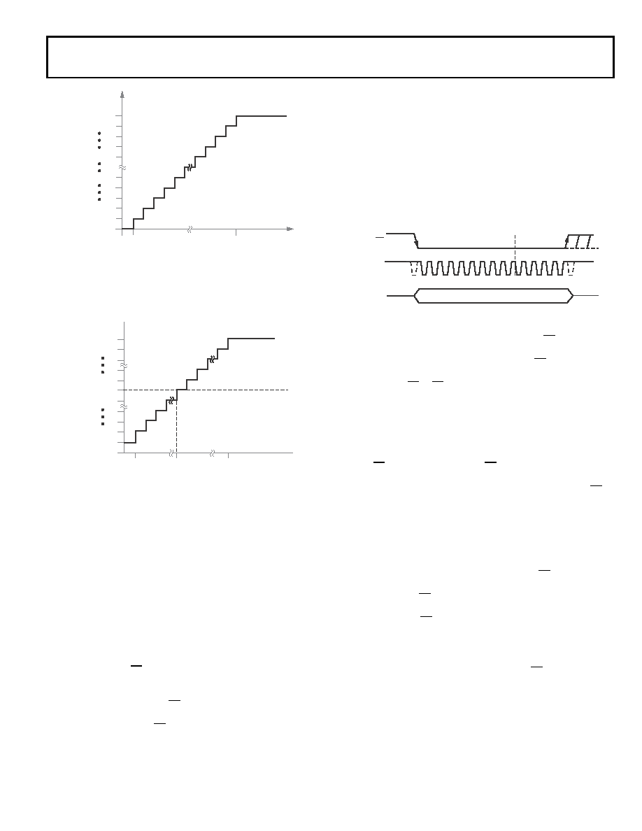
Figure 78. Straight Binary Transfer Characteristic
Figure 79. Twos Complement Transfer Characteristic with
VREF ± VREF Input Range
000...000
111...111
1LSB = VREF/4096
1LSB
VREF – 1LSB
ANALOG INPUT
ADC
CODE
0V
000...001
000...010
111...110
111...000
011...111
NOTE
1. VREF IS EITHER VREF OR 2 × VREF.
100...000
011...111
1LSB = 2
u V
REF/4096
+VREF – 1 LSB
–VREF + 1LSB VREF – 1LSB
ANALOG INPUT
ADC
CODE
100...001
100...010
011...110
000...001
000...000
111...111
Figure 80. Normal Mode Operation
ADSCLK
LEADING ZEROS + CONVERSION RESULT
CS
DOUTA
DOUTB
114
10
相关PDF资料 |
PDF描述 |
|---|---|
| TPSB476K010H0500 | CAP TANT 47UF 10V 10% 1210 |
| GBC08DREN | CONN EDGECARD 16POS .100 EYELET |
| CS48540-DQZR | IC DSP HP 32BIT 8CH I/O 48-QFP |
| 2300HT-220-V-RC | INDUCTOR TOROID 22UH 15% VERT |
| JWT75-5FF/A | PS TRIPLE OUTPUT +5V/+15V/-15V |
相关代理商/技术参数 |
参数描述 |
|---|---|
| ADSP-BF506BSWZ-3F | 功能描述:IC DSP 400MHZ 1.4V 120LQFP RoHS:是 类别:集成电路 (IC) >> 嵌入式 - DSP(数字式信号处理器) 系列:Blackfin® 标准包装:40 系列:TMS320DM64x, DaVinci™ 类型:定点 接口:I²C,McASP,McBSP 时钟速率:400MHz 非易失内存:外部 芯片上RAM:160kB 电压 - 输入/输出:3.30V 电压 - 核心:1.20V 工作温度:0°C ~ 90°C 安装类型:表面贴装 封装/外壳:548-BBGA,FCBGA 供应商设备封装:548-FCBGA(27x27) 包装:托盘 配用:TMDSDMK642-0E-ND - DEVELPER KIT W/NTSC CAMERA296-23038-ND - DSP STARTER KIT FOR TMS320C6416296-23059-ND - FLASHBURN PORTING KIT296-23058-ND - EVAL MODULE FOR DM642TMDSDMK642-ND - DEVELOPER KIT W/NTSC CAMERA |
| ADSP-BF506BSWZ-4F | 功能描述:IC DSP 400MHZ 1.4V 120LQFP RoHS:是 类别:集成电路 (IC) >> 嵌入式 - DSP(数字式信号处理器) 系列:Blackfin® 标准包装:40 系列:TMS320DM64x, DaVinci™ 类型:定点 接口:I²C,McASP,McBSP 时钟速率:400MHz 非易失内存:外部 芯片上RAM:160kB 电压 - 输入/输出:3.30V 电压 - 核心:1.20V 工作温度:0°C ~ 90°C 安装类型:表面贴装 封装/外壳:548-BBGA,FCBGA 供应商设备封装:548-FCBGA(27x27) 包装:托盘 配用:TMDSDMK642-0E-ND - DEVELPER KIT W/NTSC CAMERA296-23038-ND - DSP STARTER KIT FOR TMS320C6416296-23059-ND - FLASHBURN PORTING KIT296-23058-ND - EVAL MODULE FOR DM642TMDSDMK642-ND - DEVELOPER KIT W/NTSC CAMERA |
| ADSP-BF506BSWZ-4FX | 制造商:Analog Devices 功能描述:- Trays |
| ADSP-BF506F | 制造商:Analog Devices 功能描述:LOW POWER BLACKFIN WITH ADVANCED EMBEDDED CONNECTIVITY - Bulk |
| ADSPBF506FBSWZ-ENG | 制造商:Analog Devices 功能描述:- Trays |
发布紧急采购,3分钟左右您将得到回复。