- 您现在的位置:买卖IC网 > PDF目录19403 > ADSP-BF504KCPZ-4F (Analog Devices Inc)IC CCD SIGNAL PROCESSOR 88LFCSP PDF资料下载
参数资料
| 型号: | ADSP-BF504KCPZ-4F |
| 厂商: | Analog Devices Inc |
| 文件页数: | 61/80页 |
| 文件大小: | 0K |
| 描述: | IC CCD SIGNAL PROCESSOR 88LFCSP |
| 视频文件: | Blackfin? BF50x Processor Family |
| 标准包装: | 1 |
| 系列: | Blackfin® |
| 类型: | 定点 |
| 接口: | CAN,EBI/EMI,I²C,IrDA,PPI,SPI,SPORT,UART/USART |
| 时钟速率: | 400MHz |
| 非易失内存: | 闪存(16MB) |
| 芯片上RAM: | 68kB |
| 电压 - 输入/输出: | 3.30V |
| 电压 - 核心: | 1.31V |
| 工作温度: | 0°C ~ 70°C |
| 安装类型: | 表面贴装 |
| 封装/外壳: | 88-VFQFN 裸露焊盘,CSP |
| 供应商设备封装: | 88-LFCSP(12x12) |
| 包装: | 托盘 |
第1页第2页第3页第4页第5页第6页第7页第8页第9页第10页第11页第12页第13页第14页第15页第16页第17页第18页第19页第20页第21页第22页第23页第24页第25页第26页第27页第28页第29页第30页第31页第32页第33页第34页第35页第36页第37页第38页第39页第40页第41页第42页第43页第44页第45页第46页第47页第48页第49页第50页第51页第52页第53页第54页第55页第56页第57页第58页第59页第60页当前第61页第62页第63页第64页第65页第66页第67页第68页第69页第70页第71页第72页第73页第74页第75页第76页第77页第78页第79页第80页
Rev. A
|
Page 64 of 80
|
July 2011
ADSP-BF504/ADSP-BF504F/ADSP-BF506F
supply using the 0 to VREF range or 2 × VREF range, respectively.
The common mode must be in this range to guarantee the func-
tionality of the ADC.
When a conversion takes place, the common mode is rejected,
resulting in a virtually noise free signal of amplitude –VREF to
+VREF corresponding to the digital codes of 0 to 4096. If the 2 ×
VREF range is used, then the input signal amplitude extends from
– 2 VREF to +2 VREF after conversion.
Driving Differential Inputs
Differential operation requires that VIN+ and VIN– be simultane-
ously driven with two equal signals that are 180° out of phase.
The common mode must be set up externally. The common-
mode range is determined by VREF, the power supply, and the
particular amplifier used to drive the analog inputs. Differential
modes of operation with either an ac or dc input provide the
best THD performance over a wide frequency range. Because
not all applications have a signal preconditioned for differential
operation, there is often a need to perform single-ended-to-dif-
ferential conversion.
Using an Op Amp Pair
An op amp pair can be used to directly couple a differential sig-
nal to one of the analog input pairs of the ADC. The circuit
configurations illustrated in Figure 72 (Dual Op Amp Circuit to
how a dual op amp can be used to convert a single-ended signal
into a differential signal for both a bipolar and unipolar input
signal, respectively.
The voltage applied to Point A sets up the common-mode volt-
age. In both diagrams, it is connected in some way to the
reference, but any value in the common-mode range can be
input here to set up the common mode. The AD8022 is a suit-
able dual op amp that can be used in this configuration to
provide differential drive to the ADC.
Take care when choosing the op amp; the selection depends on
the required power supply and system performance objectives.
The driver circuits in Figure 72 (Dual Op Amp Circuit to Con-
Bipolar Signal into a Differential Unipolar Signal) are optimized
for dc coupling applications requiring best distortion
performance.
The circuit configuration shown in Figure 72 (Dual Op Amp
ential Signal) converts a unipolar, single-ended signal into a
differential signal.
Differential Unipolar Signal) is configured to convert and level
shift a single-ended, ground-referenced (bipolar) signal to a dif-
ferential signal centered at the VREF level of the ADC.
Pseudo Differential Mode
The ADC can have a total of six pseudo differential pairs. In this
mode, VIN+ is connected to the signal source that must have an
amplitude of VREF (or 2 × VREF, depending on the range chosen)
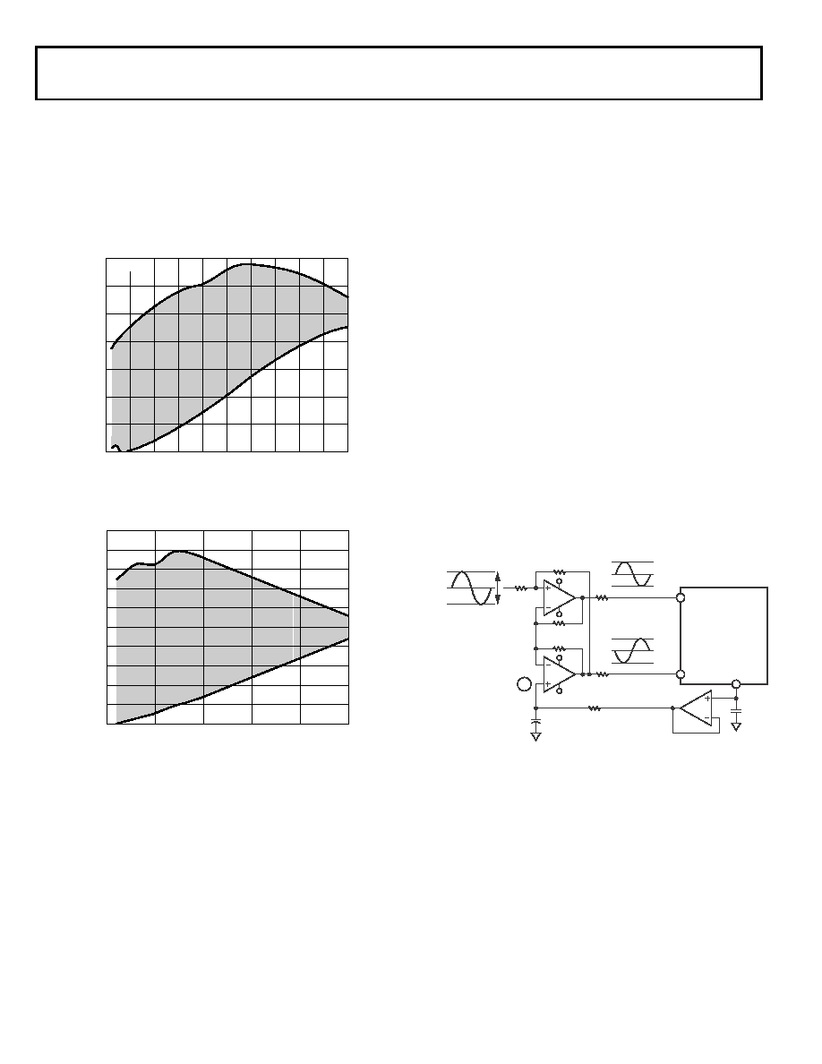
Figure 70. Input Common-Mode Range vs. VREF (0 to VREF Range, VDD = 5 V)
Figure 71. Input Common-Mode Range vs. VREF (2 × VREF Range, VDD = 5 V)
VREF (V)
5.0
0
0.5
1.0
1.5
2.0
2.5
3.0
3.5
4.0
4.5
COMMON-MODE
RANGE
(V)
3.5
3.0
2.5
2.0
1.5
1.0
0.5
0
TA = 25°C
VREF (V)
2.5
0
0.5
1.0
1.5
2.0
COMMON-MODE
RANGE
(V)
5.0
4.0
4.5
3.0
3.5
2.0
2.5
0.5
1.0
1.5
0
TA = 25°C
Figure 72. Dual Op Amp Circuit to Convert a Single-Ended Unipolar Signal
Into a Differential Signal
GND
2 × VREF p–p
27
V+
V–
V+
V–
VREF
2.5V
3.75V
1.25V
2.5V
3.75V
1.25V
VREF
(DCAPA/DCAPB)
VIN+
ADC
1
VIN–
440
220
0.47μF
1ADDITIONAL PINS OMITTED FOR CLARITY.
220
10k
A
相关PDF资料 |
PDF描述 |
|---|---|
| TPSB476K010H0500 | CAP TANT 47UF 10V 10% 1210 |
| GBC08DREN | CONN EDGECARD 16POS .100 EYELET |
| CS48540-DQZR | IC DSP HP 32BIT 8CH I/O 48-QFP |
| 2300HT-220-V-RC | INDUCTOR TOROID 22UH 15% VERT |
| JWT75-5FF/A | PS TRIPLE OUTPUT +5V/+15V/-15V |
相关代理商/技术参数 |
参数描述 |
|---|---|
| ADSP-BF506BSWZ-3F | 功能描述:IC DSP 400MHZ 1.4V 120LQFP RoHS:是 类别:集成电路 (IC) >> 嵌入式 - DSP(数字式信号处理器) 系列:Blackfin® 标准包装:40 系列:TMS320DM64x, DaVinci™ 类型:定点 接口:I²C,McASP,McBSP 时钟速率:400MHz 非易失内存:外部 芯片上RAM:160kB 电压 - 输入/输出:3.30V 电压 - 核心:1.20V 工作温度:0°C ~ 90°C 安装类型:表面贴装 封装/外壳:548-BBGA,FCBGA 供应商设备封装:548-FCBGA(27x27) 包装:托盘 配用:TMDSDMK642-0E-ND - DEVELPER KIT W/NTSC CAMERA296-23038-ND - DSP STARTER KIT FOR TMS320C6416296-23059-ND - FLASHBURN PORTING KIT296-23058-ND - EVAL MODULE FOR DM642TMDSDMK642-ND - DEVELOPER KIT W/NTSC CAMERA |
| ADSP-BF506BSWZ-4F | 功能描述:IC DSP 400MHZ 1.4V 120LQFP RoHS:是 类别:集成电路 (IC) >> 嵌入式 - DSP(数字式信号处理器) 系列:Blackfin® 标准包装:40 系列:TMS320DM64x, DaVinci™ 类型:定点 接口:I²C,McASP,McBSP 时钟速率:400MHz 非易失内存:外部 芯片上RAM:160kB 电压 - 输入/输出:3.30V 电压 - 核心:1.20V 工作温度:0°C ~ 90°C 安装类型:表面贴装 封装/外壳:548-BBGA,FCBGA 供应商设备封装:548-FCBGA(27x27) 包装:托盘 配用:TMDSDMK642-0E-ND - DEVELPER KIT W/NTSC CAMERA296-23038-ND - DSP STARTER KIT FOR TMS320C6416296-23059-ND - FLASHBURN PORTING KIT296-23058-ND - EVAL MODULE FOR DM642TMDSDMK642-ND - DEVELOPER KIT W/NTSC CAMERA |
| ADSP-BF506BSWZ-4FX | 制造商:Analog Devices 功能描述:- Trays |
| ADSP-BF506F | 制造商:Analog Devices 功能描述:LOW POWER BLACKFIN WITH ADVANCED EMBEDDED CONNECTIVITY - Bulk |
| ADSPBF506FBSWZ-ENG | 制造商:Analog Devices 功能描述:- Trays |
发布紧急采购,3分钟左右您将得到回复。