- 您现在的位置:买卖IC网 > PDF目录19403 > ADSP-BF504KCPZ-4F (Analog Devices Inc)IC CCD SIGNAL PROCESSOR 88LFCSP PDF资料下载
参数资料
| 型号: | ADSP-BF504KCPZ-4F |
| 厂商: | Analog Devices Inc |
| 文件页数: | 8/80页 |
| 文件大小: | 0K |
| 描述: | IC CCD SIGNAL PROCESSOR 88LFCSP |
| 视频文件: | Blackfin? BF50x Processor Family |
| 标准包装: | 1 |
| 系列: | Blackfin® |
| 类型: | 定点 |
| 接口: | CAN,EBI/EMI,I²C,IrDA,PPI,SPI,SPORT,UART/USART |
| 时钟速率: | 400MHz |
| 非易失内存: | 闪存(16MB) |
| 芯片上RAM: | 68kB |
| 电压 - 输入/输出: | 3.30V |
| 电压 - 核心: | 1.31V |
| 工作温度: | 0°C ~ 70°C |
| 安装类型: | 表面贴装 |
| 封装/外壳: | 88-VFQFN 裸露焊盘,CSP |
| 供应商设备封装: | 88-LFCSP(12x12) |
| 包装: | 托盘 |
第1页第2页第3页第4页第5页第6页第7页当前第8页第9页第10页第11页第12页第13页第14页第15页第16页第17页第18页第19页第20页第21页第22页第23页第24页第25页第26页第27页第28页第29页第30页第31页第32页第33页第34页第35页第36页第37页第38页第39页第40页第41页第42页第43页第44页第45页第46页第47页第48页第49页第50页第51页第52页第53页第54页第55页第56页第57页第58页第59页第60页第61页第62页第63页第64页第65页第66页第67页第68页第69页第70页第71页第72页第73页第74页第75页第76页第77页第78页第79页第80页
Rev. A
|
Page 16 of 80
|
July 2011
ADSP-BF504/ADSP-BF504F/ADSP-BF506F
All on-chip peripherals are clocked by the system clock (SCLK).
The system clock frequency is programmable by means of the
SSEL3–0 bits of the PLL_DIV register. The values programmed
into the SSEL fields define a divide ratio between the PLL output
(VCO) and the system clock. SCLK divider values are 1 through
15. Table 6 illustrates typical system clock ratios.
Note that the divisor ratio must be chosen to limit the system
clock frequency to its maximum of fSCLK. The SSEL value can be
changed dynamically without any PLL lock latencies by writing
the appropriate values to the PLL divisor register (PLL_DIV).
The core clock (CCLK) frequency can also be dynamically
changed by means of the CSEL1–0 bits of the PLL_DIV register.
Supported CCLK divider ratios are 1, 2, 4, and 8, as shown in
Table 7. This programmable core clock capability is useful for
fast core frequency modifications.
The maximum CCLK frequency both depends on the part’s
speed grade and depends on the applied VDDINT voltage. See
Table 14 for details. The maximal system clock rate (SCLK)
depends on the applied VDDINT and VDDEXT voltages (see
BOOTING MODES
The processor has several mechanisms (listed in Table 8) for
automatically loading internal and external memory after a
reset. The boot mode is defined by the BMODE input pins dedi-
cated to this purpose. There are two categories of boot modes.
In master boot modes, the processor actively loads data from
parallel or serial memories. In slave boot modes, the processor
receives data from external host devices.
The boot modes listed in Table 8 provide a number of mecha-
nisms for automatically loading the processor’s internal and
external memories after a reset. By default, all boot modes use
the slowest meaningful configuration settings. Default settings
can be altered via the initialization code feature at boot time.
Some boot modes require a boot host wait (HWAIT) signal,
which is a GPIO output signal that is driven and toggled by the
boot kernel at boot time. If pulled high through an external pull-
up resistor, the HWAIT signal behaves active high and will be
driven low when the processor is ready for data. Conversely,
when pulled low, HWAIT is driven high when the processor is
ready for data. When the boot sequence completes, the HWAIT
pin can be used for other purposes. The BMODE pins of the
reset configuration register, sampled during power-on resets
and software-initiated resets, implement the modes shown in
IDLE State / No Boot (BMODE = 0x0)—In this mode, the
boot kernel transitions the processor into Idle state. The
processor can then be controlled through JTAG for recov-
ery, debug, or other functions.
Boot from stacked parallel flash in 16-bit asynchronous
mode (BMODE = 0x1)—In this mode, conservative timing
parameters are used to communicate with the flash device.
The boot kernel communicates with the flash device
asynchronously.
Boot from stacked parallel flash in 16-bit synchronous
mode (BMODE = 0x2)—In this mode, fast timing parame-
ters are used to communicate with the flash device. The
boot kernel configures the flash device for synchronous
burst communication and boots from the flash
synchronously.
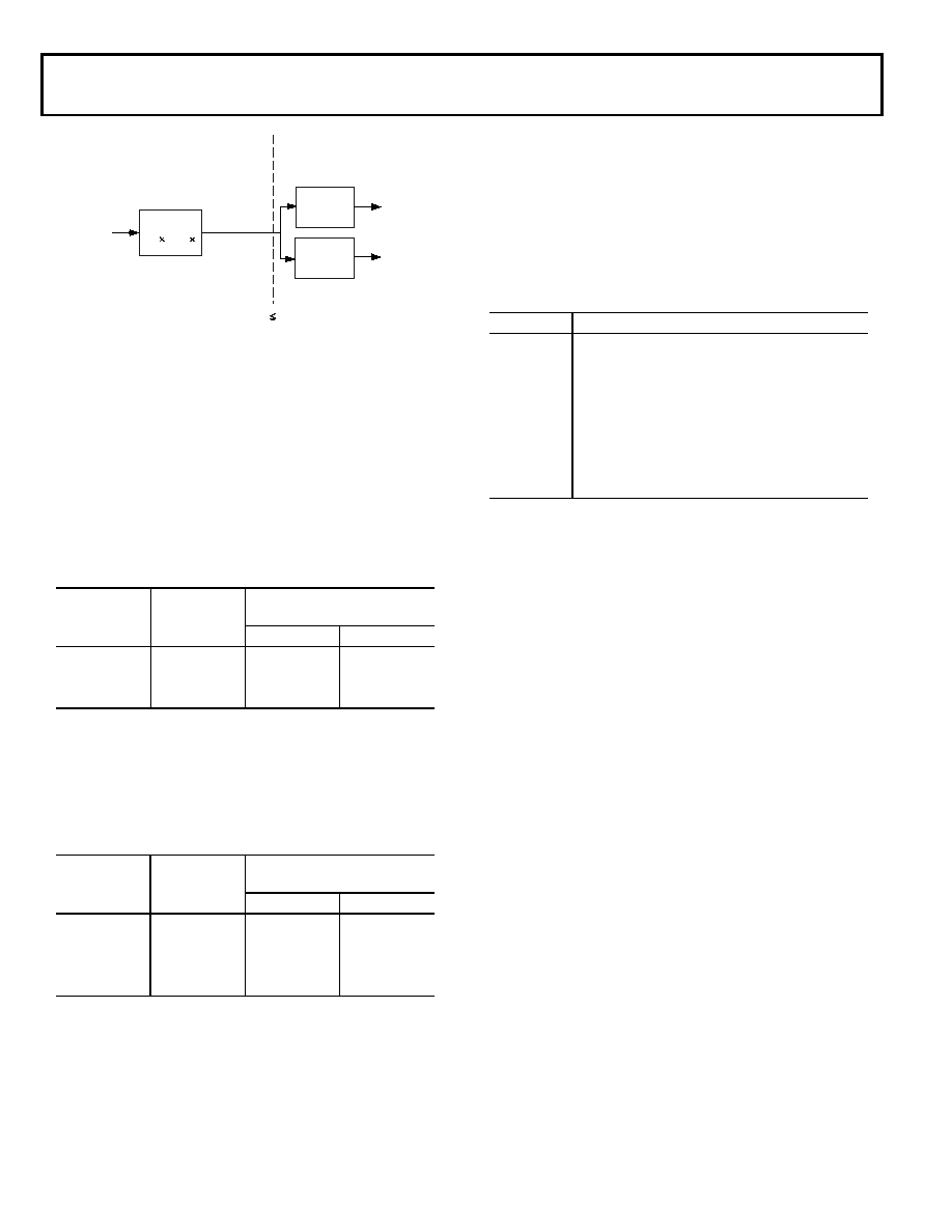
Figure 5. Frequency Modification Methods
Table 6. Example System Clock Ratios
Signal Name
SSEL3–0
Divider Ratio
VCO/SCLK
Example Frequency Ratios
(MHz)
VCO
SCLK
0001
1:1
50
0110
6:1
300
50
1010
10:1
400
40
Table 7. Core Clock Ratios
Signal Name
CSEL1–0
Divider Ratio
VCO/CCLK
Example Frequency Ratios
(MHz)
VCO
CCLK
00
1:1
300
01
2:1
300
150
10
4:1
400
100
11
8:1
200
25
PLL
0.5
u to 64u
÷1 to 15
÷1, 2, 4, 8
VCO
CLKIN
“FINE” ADJUSTMENT
REQUIRES PLL SEQUENCING
“COARSE” ADJUSTMENT
ON-THE-FLY
CCLK
SCLK
d CCLK
Table 8. Booting Modes
BMODE2–0 Description
000
Idle/No Boot
001
Boot from internal parallel flash in async mode1
1 This boot mode applies to ADSP-BF504F and ADSP-BF506F processors only.
010
Boot from internal parallel flash in sync mode1
011
Boot through SPI0 master from SPI memory
100
Boot through SPI0 slave from host device
101
Boot through PPI from host
110
Reserved
111
Boot through UART0 slave from host device
相关PDF资料 |
PDF描述 |
|---|---|
| TPSB476K010H0500 | CAP TANT 47UF 10V 10% 1210 |
| GBC08DREN | CONN EDGECARD 16POS .100 EYELET |
| CS48540-DQZR | IC DSP HP 32BIT 8CH I/O 48-QFP |
| 2300HT-220-V-RC | INDUCTOR TOROID 22UH 15% VERT |
| JWT75-5FF/A | PS TRIPLE OUTPUT +5V/+15V/-15V |
相关代理商/技术参数 |
参数描述 |
|---|---|
| ADSP-BF506BSWZ-3F | 功能描述:IC DSP 400MHZ 1.4V 120LQFP RoHS:是 类别:集成电路 (IC) >> 嵌入式 - DSP(数字式信号处理器) 系列:Blackfin® 标准包装:40 系列:TMS320DM64x, DaVinci™ 类型:定点 接口:I²C,McASP,McBSP 时钟速率:400MHz 非易失内存:外部 芯片上RAM:160kB 电压 - 输入/输出:3.30V 电压 - 核心:1.20V 工作温度:0°C ~ 90°C 安装类型:表面贴装 封装/外壳:548-BBGA,FCBGA 供应商设备封装:548-FCBGA(27x27) 包装:托盘 配用:TMDSDMK642-0E-ND - DEVELPER KIT W/NTSC CAMERA296-23038-ND - DSP STARTER KIT FOR TMS320C6416296-23059-ND - FLASHBURN PORTING KIT296-23058-ND - EVAL MODULE FOR DM642TMDSDMK642-ND - DEVELOPER KIT W/NTSC CAMERA |
| ADSP-BF506BSWZ-4F | 功能描述:IC DSP 400MHZ 1.4V 120LQFP RoHS:是 类别:集成电路 (IC) >> 嵌入式 - DSP(数字式信号处理器) 系列:Blackfin® 标准包装:40 系列:TMS320DM64x, DaVinci™ 类型:定点 接口:I²C,McASP,McBSP 时钟速率:400MHz 非易失内存:外部 芯片上RAM:160kB 电压 - 输入/输出:3.30V 电压 - 核心:1.20V 工作温度:0°C ~ 90°C 安装类型:表面贴装 封装/外壳:548-BBGA,FCBGA 供应商设备封装:548-FCBGA(27x27) 包装:托盘 配用:TMDSDMK642-0E-ND - DEVELPER KIT W/NTSC CAMERA296-23038-ND - DSP STARTER KIT FOR TMS320C6416296-23059-ND - FLASHBURN PORTING KIT296-23058-ND - EVAL MODULE FOR DM642TMDSDMK642-ND - DEVELOPER KIT W/NTSC CAMERA |
| ADSP-BF506BSWZ-4FX | 制造商:Analog Devices 功能描述:- Trays |
| ADSP-BF506F | 制造商:Analog Devices 功能描述:LOW POWER BLACKFIN WITH ADVANCED EMBEDDED CONNECTIVITY - Bulk |
| ADSPBF506FBSWZ-ENG | 制造商:Analog Devices 功能描述:- Trays |
发布紧急采购,3分钟左右您将得到回复。